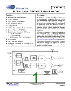
CS4351
6.3.4 ATAPI Channel Mixing and Muting (ATAPI3:0) Bits 3-0 .................................................. 26
6.4 Mute Control - Register 04h ........................................................................................................ 27
6.4.1 Auto-Mute (AMUTE) Bit 7 ................................................................................................ 27
6.4.2 AMUTEC = BMUTEC (MUTEC A=B) Bit 5 ...................................................................... 27
6.4.3 A Channel Mute (MUTE_A) Bit 4
B Channel Mute (MUTE_B) Bit 3 .................................................................................... 27
6.5 Channel A Volume Control - Register 05h
Channel B Volume Control - Register 06h ................................................................................ 27
6.5.1 Digital Volume Control (VOL7:0) Bits 7-0 ........................................................................ 28
6.6 Ramp and Filter Control - Register 07h ........................................................................................ 28
6.6.1 Soft Ramp and Zero Cross Control (SZC1:0) Bits 7-6 ..................................................... 28
6.6.2 Soft Volume Ramp-Up After Error (RMP_UP) Bit 5 ......................................................... 29
6.6.3 Soft Ramp-Down Before Filter Mode Change (RMP_DN) Bit 4 ....................................... 29
6.6.4 Interpolation Filter Select (FILT_SEL) Bit 2 ..................................................................... 29
6.7 Misc Control - Register 08h .......................................................................................................... 29
6.7.1 Power Down (PDN) Bit 7 ................................................................................................. 30
6.7.2 Control Port Enable (CPEN) Bit 6 .................................................................................... 30
6.7.3 Freeze Controls (Freeze) Bit 5 ......................................................................................... 30
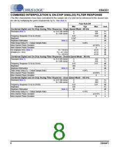
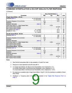
7. DIGITAL FILTER RESPONSE PLOTS ............................................................................................. 31
8. PARAMETER DEFINITIONS ............................................................................................................... 35
9. PACKAGE DIMENSIONS .................................................................................................................. 36
10. ORDERING INFORMATION ............................................................................................................. 37
11. REVISION HISTORY ......................................................................................................................... 37
LIST OF FIGURES
Figure 1. Serial Input Timing..................................................................................................................... 10
Figure 2. Control Port Timing - I²C Format................................................................................................ 11
Figure 3. Control Port Timing - SPI Format (Write)................................................................................... 12
Figure 4. Typical Connection Diagram...................................................................................................... 14
Figure 5. Left-Justified up to 24-Bit Data................................................................................................... 17
Figure 6. I²S, up to 24-Bit Data ................................................................................................................. 17
Figure 7. Right-Justified Data.................................................................................................................... 17
Figure 8. De-Emphasis Curve................................................................................................................... 17
Figure 9. Control Port Timing, I²C Mode ................................................................................................... 21
Figure 10.Control Port Timing, SPI mode .................................................................................................. 22
Figure 11.De-Emphasis Curve................................................................................................................... 24
Figure 12.ATAPI Block Diagram ................................................................................................................ 26
Figure 13.Single-Speed (fast) Stopband Rejection.................................................................................... 31
Figure 14.Single-Speed (fast) Transition Band.......................................................................................... 31
Figure 15.Single-Speed (fast) Transition Band (detail).............................................................................. 31
Figure 16.Single-Speed (fast) Passband Ripple........................................................................................ 31
Figure 17.Single-Speed (slow) Stopband Rejection .................................................................................. 31
Figure 18.Single-Speed (slow) Transition Band......................................................................................... 31
Figure 19.Single-Speed (slow) Transition Band (detail)............................................................................. 32
Figure 20.Single-Speed (slow) Passband Ripple....................................................................................... 32
Figure 21.Double-Speed (fast) Stopband Rejection .................................................................................. 32
Figure 22.Double-Speed (fast) Transition Band......................................................................................... 32
Figure 23.Double-Speed (fast) Transition Band (detail)............................................................................. 32
Figure 24.Double-Speed (fast) Passband Ripple....................................................................................... 32
Figure 25.Double-Speed (slow) Stopband Rejection................................................................................. 33
Figure 26.Double-Speed (slow) Transition Band ....................................................................................... 33
Figure 27.Double-Speed (slow) Transition Band (detail) ........................................................................... 33
Figure 28.Double-Speed (slow) Passband Ripple ..................................................................................... 33
DS566F1
3

 CIRRUS [ CIRRUS LOGIC ]