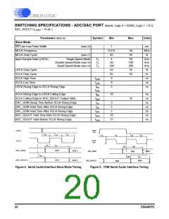
Parameters (Note 20)
Symbol
Min
Max
Units
Master Mode
Output Sample Rate (LRCK)
LRCK Duty Cycle
All Speed Modes
F
-
45
-
MCLK / 256
kHz
%
s
55
SCLK Frequency
64 x Fs
MHz
%
SCLK Duty Cycle
45
-
55
5
LRCK Edge to SCLK Rising Edge
t
ns
lcks
SCLK Falling Edge to ADC_SDOUT Output Valid
DAC_SDIN Setup Time Before SCLK Rising Edge
DAC_SDIN Hold Time After SCLK Rising Edge
t
-
35
-
ns
dpd
t
3
ns
ds
t
5
-
ns
dh1
Notes: 16. After powering up the CS42448, RST should be held low after the power supplies and clocks are settled.
17. See Table 10 on page 46 and Table 11 on page 47 for suggested MCLK frequencies.
18. When operating in TDM interface format, VLS is limited to nominal 2.5 V to 5.0 V operation only.
19. ADC - I²S, Left-Justified, Right-Justified interface formats only. DAC - I²S, Left-Justified, Right-Justified
and Time Division Multiplexed interface formats only.
20. “LRCK” and “SCLK” shall refer to the ADC and DAC left/right clock and serial clock, respectively.
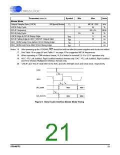
LRCK
tlcks
SCLK
tds
tdh
DAC_SDINx
MSB
MSB
MSB-1
MSB-1
tdpd
ADC_SDOUTx
Figure 6. Serial Audio Interface Master Mode Timing
DS648PP2
21

 CIRRUS [ CIRRUS LOGIC ]