Applications Information: continued
4. Connect the ground terminals of the Compensation
7. If DC regulation is to be optimized (at the expense of
degraded transient regulation), adaptive voltage position-
ing can be disabled by connecting to VFB pin directly to the
load with a separate trace (remote sense).
capacitor directly to the ground of the fast feedback filter
capacitor to prevent common mode noise from effecting
the PWM comparator.
5. Place the output filter capacitor(s) as close to the load as
8. Place 5V input capacitors close to the switching MOSFET
possible and connect the ground terminal to pin 14 (LGnd). and synchronous MOSFET.
6. To implement adaptive voltage positioning, connect
both slow and fast feedback pins 16 (VFB) and 8 (VFFB) to
Route gate drive signals VGATE(H) (pin 10) and VGATE(L)
(pin 12 when used) with traces that are a minimum of 0.025
the regulator output right at the inductor terminal. Connect inches wide.
inductor to the output capacitors via a trace with the fol-
lowing resistance:
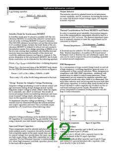
VCC
To the negative terminal of the
0.1µF
input capacitors
15
11
80mV
IMAX
RTRACE
=
1.0µF
V
COMP
100pF
FFB
This causes the output voltage to be +40mV with no load,
and -40mV with a full load, improving regulator transient
response. This trace must be wide enough to carry the full
output current. (Typical trace is 1.0 inch long, 0.17 inch
wide). Care should be taken to minimize any additional
losses after the feedback connection point to maximize reg-
ulation.
V
8
5
SOFTSTART
OFF TIME
To the negative terminal of the output capacitors
Figure 20: Layout Guidelines
Additional Application Circuits
5V
3.3V
12V
1µF
0.1µF
MBRS120
1µF
MBRS120
MBRS
120
+
33µF/25V x 3
+
100µF/10V x 3
Tantalum
1µF
Tantalum
Si9410
Si4410DY
VCC2
VCC1
VID0
VGATE(H)
V
CC2
V
5µH
V
CC1
GATE(H)
2.5V/7A
3µH
3.3V/10A
V
ID0
VID1
VID2
V
V
ID1
VFB
+
ID2
100µF/10V x 2
CS5155H
CS5155H
VID3
VID4
COFF
V
ID3
V
ID4
Tantalum
Si9410DY
V
GATE(L)
Si9410
VGATE(L)
C
OFF
PGnd
330pF
330pF
SS
SS
V
PGnd
VFFB
FB
0.1µF
3.3k
COMP
0.1µF
3.3k
COMP
V
LGnd
FFB
LGnd
0.33µF
+
0.33µF
100pF
100µF/10V x 3
100pF
Tantalum
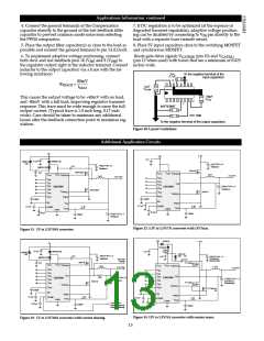
Figure 23: 3.3V to 2.5V/7A converter with 12V bias.
Figure 21: 5V to 3.3V/10A converter.
12V
1N5818
+12V
5V
1N5818
22Ω
0.1µF
MBRS120
1µF
MBRS120
1µF
1/4W
MBRS
120
1N4746
18V 1W
+
+
100µF/10V x 3
Tantalum
1µF
1µF
820µF/16V × 4
Aluminum
0.1µF
Remote
Sense
Electrolytic
Si4410
FY10AAJ-
V
CC2
V
V
GATE(H)
VCC2
03
CC1
VCC1
VID0
VGATE(H)
3µH
1.1µH
3.3V/10A
3.3V/5A
V
ID0
V
V
ID1
ID2
VID1
VID2
V
FB
VFB
10Ω
+
CS5155H
CS5155H
100µF/10V x 3
Tantalum
+
1200µF/10V × 2
Aluminum
Electrolytic
V
V
ID3
VID3
VID4
COFF
Si9410
FY10AAJ-
03
ID4
V
GATE(L)
VGATE(L)
C
OFF
FY10AAJ-
03
330pF
330pF
SS
SS
PGnd
PGnd
VFFB
3.3k
0.1µF
COMP
0.1µF
3.3k
COMP
V
FFB
LGnd
LGnd
Connect to
other circuits for
current sharing
0.33µF
100pF
0.33µF
100pF
Figure 24: 12V to 3.3V/5A converter with remote sense.
Figure 22: 5V to 3.3V/10A converter with current sharing.
13

 CHERRY [ CHERRY SEMICONDUCTOR CORPORATION ]