Applications Information: continued
Output Inductor
COFF timing capacitor:
The inductor should be selected based on its inductance,
Period × (1 - duty cycle)
current capability, and DC resistance. Increasing the induc-
tor value will decrease output voltage ripple, but degrade
transient response.
COFF
=
,
4848.5
where:
1
Period =
Thermal Management
switching frequency
Thermal Considerations for Power MOSFETs and Diodes
In order to maintain good reliability, the junction tempera-
ture of the semiconductor components should be kept to a
maximum of 150°C or lower. The thermal impedance (junc-
tion to ambient) required to meet this requirement can be
calculated as follows:
Schottky Diode for Synchronous MOSFET
A Schottky diode may be placed in parallel with the syn-
chronous MOSFET to conduct the inductor current upon
turn off of the switching MOSFET to improve efficiency.
The CS5155H reference circuit does not use this device due
to it’s excellent design. Instead, the body diode of the syn-
chronous MOSFET is utilized to reduce cost and conducts
the inductor current. For a design operating at 200kHz or so,
the low non-overlap time combined with Schottky forward
recovery time may make the benefits of this device not
worth the additional expense (see Figure 6, channel 2). The
power dissipation in the synchronous MOSFET due to body
diode conduction can be estimated by the following equation:
TJUNCTION(MAX) - TAMBIENT
Thermal Impedance =
Power
A heatsink may be added to TO-220 components to reduce
their thermal impedance. A number of PC board layout
techniques such as thermal vias and additional copper foil
area can be used to improve the power handling capability
of surface mount components.
Power = Vbd × ILOAD × conduction time × switching frequency
EMI Management
As a consequence of large currents being turned on and off
at high frequency, switching regulators generate noise as a
consequence of their normal operation. When designing for
compliance with EMI/EMC regulations, additional com-
ponents may be added to reduce noise emissions. These
components are not required for regulator operation and
experimental results may allow them to be eliminated. The
input filter inductor may not be required because bulk filter
and bypass capacitors, as well as other loads located on the
board will tend to reduce regulator di/dt effects on the cir-
cuit board and input power supply. Placement of the
power component to minimize routing distance will also
help to reduce emissions.
Where Vbd = the forward drop of the MOSFET body diode.
For the CS5155H demonstration board as shown in Figure 6;
Power = 1.6V × 13A × 100ns × 233kHz = 0.48W
This is only 1.3% of the 36.4W being delivered to the load.
“Droop” Resistor for Adaptive Voltage Positioning
Adaptive voltage positioning is used to reduce output volt-
age excursions during abrupt changes in load current.
Regulator output voltage is offset +40mV when the regula-
tor is unloaded, and -40mV at full load. This results in
increased margin before encountering minimum and maxi-
mum transient voltage limits, allowing use of less capaci-
tance on the regulator output (see Figure 7).
To implement adaptive voltage positioning, a “droop”
resistor must be connected between the output inductor
and output capacitors and load. This is normally imple-
mented by a PC board trace of the following value:
2µH
2µH
+
80mV
IMAX
1200µF x 3/16V
33Ω
RDROOP
=
1000pF
Adaptive voltage positioning can be disabled for improved
DC regulation by connecting the VFB pin directly to the load
using a separate, non-load current carrying circuit trace.
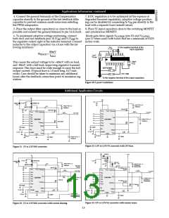
Figure 18: Filter components
Figure 19: Input Filter
Input and Output Capacitors
Layout Guidelines
These components must be selected and placed carefully to
yield optimal results. Capacitors should be chosen to pro-
vide acceptable ripple on the input supply lines and regula-
tor output voltage. Key specifications for input capacitors
are their ripple rating, while ESR is important for output
capacitors. For best transient response, a combination of
low value/high frequency and bulk capacitors placed close
to the load will be required.
1. Place 12V filter capacitor next to the IC and connect
capacitor ground to pin 11 (PGnd).
2. Connect pin 11 (PGnd) with a separate trace to the
ground terminals of the 5V input capacitors.
3. Place fast feedback filter capacitor next to pin 8 (VFFB
and connect it’s ground terminal with a separate, wide
trace directly to pin 14 (LGnd).
)
12

 CHERRY [ CHERRY SEMICONDUCTOR CORPORATION ]