CM6805BO
10-PIN Green-Mode PFC/PWM Combo CONTROLLER
PFCOFFB (Pin 7)
PFCOUT (Pin 9) and PWM OUT (Pin 10)
PFC OUT and PWM OUT are the high-current power driver
capable of directly driving the gate of a power MOSFET with
peak currents up to -1A and +0.5A. Both outputs are actively
held low when VCC is below the UVLO threshold level which
is 15V or VREFOK comparator is low.
When this pin is below 5V, PFC gate drive, PFCOUT will be
turned off until PFCOFFB pin is greater than 5.5V. When
PFCOFFB is below 5V, Veao also been pulled low as well.
PFCOFFB usually is used for AC Brown Out or Green
PWM.
For AC Brown out, PFCOFFB can be used to sense the
bridge input voltage.
For Green PWM, it can be used to sense the photo couple
current to detect the PWM load. When the load is light, the
photo couple current increased. The photo couple current
with a resistor between VCC and PFCOFFB can sense the
light load condition. When PFCOFFB is below 5V, PFC can
be turned off.
Power Factor Correction
Power factor correction makes a nonlinear load look like a
resistive load to the AC line. For a resistor, the current drawn
from the line is in phase with and proportional to the line
voltage, so the power factor is unity (one). A common class
of nonlinear load is the input of most power supplies, which
use a bridge rectifier and capacitive input filter fed from the
line. The peak-charging effect, which occurs on the input
filter capacitor in these supplies, causes brief high-amplitude
pulses of current to flow from the power line, rather than a
sinusoidal current in phase with the line voltage. Such
supplies present a power factor to the line of less than one
(i.e. they cause significant current harmonics of the power
line frequency to appear at their input). If the input current
drawn by such a supply (or any other nonlinear load) can be
made to follow the input voltage in instantaneous amplitude,
it will appear resistive to the AC line and a unity power factor
will be achieved.
VCC (Pin 8)
VCC is the power input connection to the IC. The VCC
start-up current is 100uA. The no-load ICC current is 2mA.
VCC quiescent current will include both the IC biasing
currents and the PFC and PWM output currents. Given the
operating frequency and the MOSFET gate charge (Qg),
average PFC and PWM output currents can be calculated
as IOUT = Qg x F. The average magnetizing current
required for any gate drive transformers must also be
included. The VCC pin is also assumed to be proportional
to the PFC output voltage. VCC also ties internally to the
UVLO circuitry and VREFOK comparator, enabling the IC at
13V and disabling it at 10V. VCC must be bypassed with a
high quality ceramic bypass capacitor placed as close as
possible to the IC. Good bypassing is critical to the proper
operation of the CM6805BO.
To hold the input current draw of a device drawing power
from the AC line in phase with and proportional to the input
voltage, a way must be found to prevent that device from
loading the line except in proportion to the instantaneous line
voltage. The PFC section of the CM6805BO uses a
boost-mode DC-DC converter to accomplish this. The input
to the converter is the full wave rectified AC line voltage. No
bulk filtering is applied following the bridge rectifier, so the
input voltage to the boost converter ranges (at twice line
frequency) from zero volts to the peak value of the AC input
and back to zero.
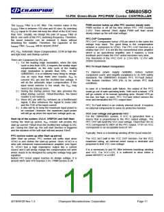
VCC is typically produced by an additional winding off the
boost inductor or PFC Choke, providing a voltage that is
proportional to the PFC output voltage. An external clamp,
such as shown in Figure 1, is desirable and proposed to
limit VCC over voltage to an acceptable value.
VCC
By forcing the boost converter to meet two simultaneous
conditions, it is possible to ensure that the current draws
from the power line matches the instantaneous line voltage.
One of these conditions is that the output voltage of the
boost converter must be set higher than the peak value of
the line voltage. A commonly used value is 385VFB, to allow
for a high line of 270VACrms. The other condition is that the
current that the converter is allowed to draw from the line at
any given instant must be proportional to the line voltage.
1N5248
GND
Figure1. Optional VCC Clamp
This limits the maximum VCC that can be applied about
18V to avoid OVP which allowing to the VCC maximum
rating. An RC filter at VCC is required between boost trap
winding and VCC.
2010/04/20 Rev 1.3
Champion Microelectronic Corporation
Page 8

 CHAMP [ CHAMPION MICROELECTRONIC CORP. ]