93C46/56/57/66/86
DEVICE OPERATION
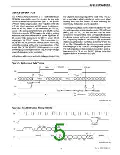
the DI pin on the rising edge of the clock (SK). The DO
pin is normally in a high impedance state except when
reading data from the device, or when checking the
ready/busy status after a write operation.
The CAT93C46/56(57)66/86 is a 1024/2048/4096/
16,384-bit nonvolatile memory intended for use with
industrystandardmicroprocessors. TheCAT93C46/56/
57/66/86 can be organized as either registers of 16 bits
or 8 bits. When organized as X16, seven 9-bit instruc-
tions for 93C46; seven 10-bit instructions for 93C57;
seven 11-bit instructions for 93C56 and 93C66; seven
13-bitinstructionsfor93C86;controlthereading, writing
and erase operations of the device. When organized as
X8, seven 10-bit instructions for 93C46; seven 11-bit
instructions for 93C57; seven 12-bit instructions for
93C56 and 93C66: seven 14-bit instructions for 93C86;
control the reading, writing and erase operations of the
device.TheCAT93C46/56/57/66/86operatesonasingle
power supply and will generate on chip, the high voltage
required during any write operation.
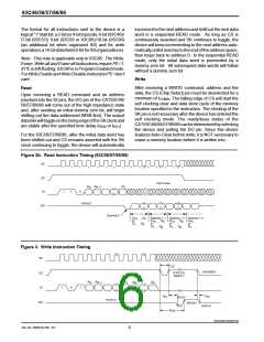
The ready/busy status can be determined after the start
ofawriteoperationbyselectingthedevice(CShigh)and
polling the DO pin; DO low indicates that the write
operation is not completed, while DO high indicates that
the device is ready for the next instruction. If necessary,
the DO pin may be placed back into a high impedance
state during chip select by shifting a dummy “1” into the
DIpin. TheDOpinwillenterthehighimpedancestateon
the falling edge of the clock (SK). Placing the DO pin into
the high impedance state is recommended in applica-
tions where the DI pin and the DO pin are to be tied
together to form a common DI/O pin.
Instructions, addresses, and write data are clocked into
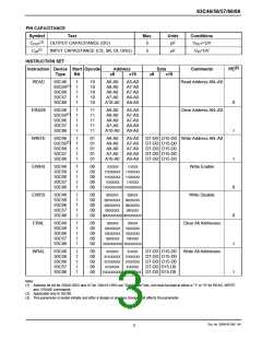
Figure 1. Sychronous Data Timing
t
t
t
SKLOW
SKHI
CSH
SK
t
t
DIS
DIH
VALID
VALID
DI
t
CSS
CS
t
t
t
t
DIS
PD0, PD1
CSMIN
DO
DATA VALID
93C46/56/57/66/86 F03
Figure 2a. Read Instruction Timing (93C46)
SK
t
CS
CS
STANDBY
A
A
A
0
N
N–1
DI
1
1
0
t
HZ
t
HIGH-Z
HIGH-Z
PD0
DO
0
D
D
D
D
0
N
N–1
1
93C46/56/57/66/86 F04
Doc. No. 25056-00 2/98 M-1
5

 CATALYST [ CATALYST SEMICONDUCTOR ]