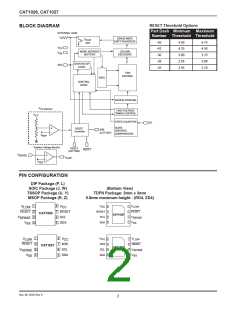
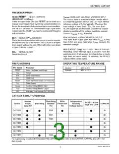
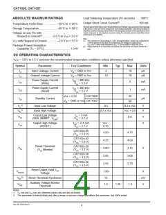
CAT1026, CAT1027
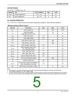
VOLTAGE MONITOR AND RESET CIRCUIT AC CHARACTERISTICS
Test
Conditions
Symbol
Parameter
Min
Typ
Max
Units
tPURST
tRPD1
tGLITCH
tWD
Reset Timeout
Note 2
130
200
270
5
ms
µs
VTH to RESET Output Delay
Note 3
VCC Glitch Reject Pulse Width
Watchdog Timeout
Note 4, 6
Note 1
30
2.1
5
ns
sec
µs
1.0
1.6
tRPD2
VSENSE to VLOW Delay
Note 5
POWER-UP TIMING6,7
Test
Conditions
Symbol
Parameter
Min
Typ
Max
Units
tPUR
tPUW
Power-Up to Read Operation
Power-Up to Write Operation
270
270
ms
ms
AC TEST CONDITIONS
Parameter
Conditions
0.2 VCC to 0.8 VCC
10 ns
Input Pulse Voltages
Input Rise and Fall Times
Input Reference Voltages
Output Reference Voltages
0.3 VCC , 0.7 VCC
0.5 VCC
Current Source: IOL = 3 mA;
CL = 100 pF
Output Load
RELIABILITY CHARACTERISTICS
Symbol
Parameter
Reference Test Method
Min
Max
Units
(6)
NEND
Endurance
MIL-STD-883, Test Method 1033 1,000,000
Cycles/Byte
Years
(6)
TDR
Data Retention
ESD Susceptibility
Latch-Up
MIL-STD-883, Test Method 1008
MIL-STD-883, Test Method 3015
JEDEC Standard 17
100
2000
100
(6)
VZAP
Volts
(6)(8)
ILTH
mA
Notes:
1. Test Conditions according to “AC Test Conditions” table.
2. Power-up, Input Reference Voltage V = V , Reset Output Reference Voltage and Load according to “AC Test Conditions” Table.
CC
TH
3. Power-Down, Input Reference Voltage V = V , Reset Output Reference Voltage and Load according to “AC Test Conditions” Table.
CC
TH
4.
V
Glitch Reference Voltage = V ; Based on characterization data.
THmin
CC
5. 0 < V
≤ V , V Output Reference Voltage and Load according to “AC Test Conditions” Table.
SENSE
CC
LOW
6. This parameter is characterized initially and after a design or process change that affects the parameter. Not 100% tested.
7. and t are the delays required from the time V is stable until the specified memory operation can be initiated.
t
PUR
PUW
CC
8. Latch-up protection is provided for stresses up to 100mA on input and output pins from -1 V to V + 1 V.
CC
Doc. No. 3010, Rev. K
6

 CATALYST [ CATALYST SEMICONDUCTOR ]