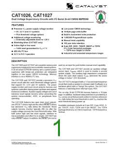
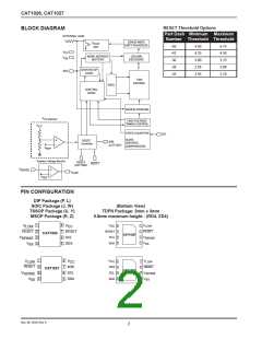
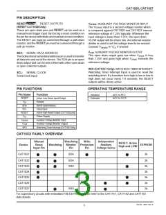
CAT1026, CAT1027
ABSOLUTE MAXIMUM RATINGS
Lead Soldering Temperature (10 seconds) ...... 300°C
Output Short Circuit Current(2) ........................ 100 mA
Temperature Under Bias ................. –55°C to +125°C
Storage Temperature....................... –65°C to +150°C
Stressesabovethoselistedunder“AbsoluteMaximumRatings”maycausepermanentdamage
to the device. These are stress ratings only, and functional operation of the device at these or
any other conditions outside of those listed in the operational sections of this specification is not
implied. Exposure to any absolute maximum rating for extended periods may affect device
performance and reliability.
Voltage on any Pin with
Respect to Ground(1) ........... –2.0 V to VCC + 2.0 V
Note:
(1) The minimum DC input voltage is –0.5V. During transitions, inputs may undershoot to
-2.0V for periods of less than 20 ns. Maximum DC voltage on output pins is
V
CC with Respect to Ground ............ –2.0 V to + 7.0 V
V
+0.5 V, which may overshoot to V +2.0V for periods of less than 20 ns.
CC
CC
Package Power Dissipation
(2) Output shorted for no more than one second. No more than one output shorted at a
Capability (TA = 25°C) .................................. 1.0 W
time.
DC OPERATING CHARACTERISTICS
V
CC
= 3.0 V to 5.5 V and over the recommended temperature conditions unless otherwise specified.
Symbol
Parameter
Test Conditions
VIN = GND to Vcc
VIN = GND to Vcc
fSCL = 400 kHz
Min
-2
Typ
Max
10
Units
µA
ILI
Input Leakage Current
Output Leakage Current
ILO
-10
10
µA
Power Supply Current
(Write)
ICC1
ICC2
3
mA
mA
V
CC = 5.5 V
Power Supply Current
(Read)
fSCL = 400 kHz
VCC = 5.5 V
1
50
Vcc = 5.5V
CAT1026
ISB
Standby Current
µA
VIN = GND or Vcc CAT1027
60
(1)
VIL
Input Low Voltage
Input High Voltage
Output Low Voltage
-0.5
0.3 x Vcc
Vcc + 0.5
V
V
(1)
VIH
0.7 x Vcc
I
OL = 3 mA
VOL
VOH
0.4
V
V
(SDA, RESET , VLOW
)
VCC = 2.7 V
Output High Voltage
(RESET)
IOH = -0.4 mA
V
Vcc -
0.75
CC = 2.7 V
CAT102x-45
(VCC = 5.0 V)
4.50
4.25
3.00
2.85
2.55
4.75
4.50
3.15
3.00
2.70
CAT102x-42
(VCC = 5.0 V)
Reset Threshold
(VCC Monitor)
CAT102x-30
(VCC = 3.3 V)
VTH
V
CAT102x-28
(VCC = 3.3 V)
CAT102x-25
(VCC = 3.0 V)
Reset Output Valid VCC
Voltage
VRVALID
1.00
15
V
mV
V
(2)
VRT
Reset Threshold Hysteresis
Auxiliary Voltage Monitor
Threshold
VREF
1.2
1.25
1.3
Notes:
1.
V
min and V max are reference values only and are not tested.
IH
IL
2. This parameter is tested initially and after a design or process change that affects the parameter. Not 100% tested.
Doc. No. 3010, Rev. K
4

 CATALYST [ CATALYST SEMICONDUCTOR ]