LH0033 / LH0033C
CORPORATION
APPLICATION INFORMATION:
Recommended Layout Precautions
where:
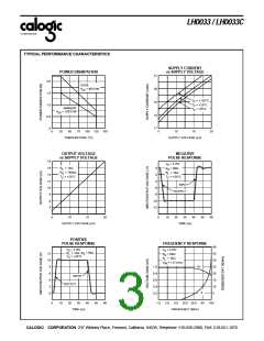
AV = No load voltage gain, typically 0.99
V+ = Positive supply voltage
V– = Negative supply voltage
RF/video printed circuit board layout rules should be followed
when using the LH0033 since it will provide power gain to
frequencies over 100MHz. Ground planes are recommended
and power supplies should be decoupled at each device with
low inductance capacitors. In addition, ground plane shielding
may be extended to the metal case of the device since it is
electrically isolated from internal circuitry. Alternatively the
case should be connected to the output to minimize input
capacitance.
For the above example, ∆VO would be -35mV. This may be
adjusted to zero as described in Figure 1. For AC coupled
applications, no additional offset occurs if the DC input is
properly biased as illustrated in the Typical Applications
section.
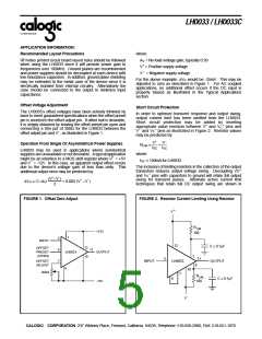
Offset Voltage Adjustment
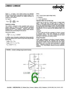
Short Circuit Protection
The LH0033’s offset voltages have been actively trimmed by
laser to meet guaranteed specifications when the offset preset
pin is shorted to the offset adjust pin. If offset null is desirable,
it is simply obtained by leaving the offset preset pin open and
connecting a trim pot of 200Ω for the LH0033 between the
offset adjust pin and V–, as illustrated in Figure 1.
In order to optimize transient response and output swing,
output current limit has been omitted from the LH0033.
Short circuit protection may be added by inserting
appropriate value resistors between V+ and VC pins and
+
V– and VC pins as illustrated in Figure 2. Resistor values
–
may be predicted by:
V+ V−
ISC ISC
Operation From Single Or Asymmetrical Power Supplies
RLIM
=
LH0033 may be used in applications where symmetrical
supplies are unavailable or not desirable. A typical application
might be an interface to a MOS shift register where V+ = +5V
and V– = -12V. In this case, an apparent output offset occurs
due to the device’s voltage gain of less than unity. This
additional output error may be predicted by:
where:
I
SC ≤ 100mA for LH0033
The inclusion of limiting resistors in the collectors of the output
transistors reduces output voltage swing. Decoupling VC+
and VC pins with capacitors to ground will retain full output
swing for transient pulses. Alternate active current limit
techniques that retain full DC output swing are shown in
–
(V+−V−)
∆VO (1−AV)
= 0.005 (V+ −V−)
2
FIGURE 1. Offset Zero Adjust
FIGURE 2. Resistor Current Limiting Using Resistor
+
V
RLIM
100
+15V
1
5
6
7
INPUT
12
C
0.1µF
12
10
OFFSET
PRESET
(OPEN)
11
LH0033
OUTPUT
1
5
11
OFFSET
ADJUST
INPUT
LH0033
OUTPUT
9
9
10
200Ω
7
RLIM
100
µ
0.1 F
6
C
-15V
-
V
CALOGIC CORPORATION, 237 Whitney Place, Fremont, California 94539, Telephone: 510-656-2900, FAX: 510-651-1076

 CALOGIC [ CALOGIC, LLC ]