Data Sheet
Input Protection
Digital Outputs
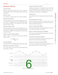
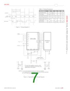
All I/O pads are protected with an on-chip protection circuit
shown in Figure 7. This circuit provides ESD robustness to
3.5kV and prevents latch-up under severe discharge con-
ditions without degrading analog transition times.
The digital outputs (D0–D10) are driven by a separate
supply (OVDD) ranging from +3 V to +5 V. This feature
makes it possible to drive the CDK1306 TTL/CMOS com-
patible outputs with the user’s logic system supply. The
format of the output data (D0–D9) is straight binary. (See
Table 3.) The outputs are latched on the rising edge of
CLK. These outputs can be switched into a tri-state mode
by bringing EN high.
Table 3. Output Data Information
Analog Input
+F.S. + 1/2 LSB
+F.S. –1/2 LSB
+1/2 F.S.
Overrange D10
Output Code D9-D0
1 1 1 1 1 1 1 1 1 1
1 1 1 1 1 1 1 1 1Ø
ØØ ØØØØ ØØØØ
0 0 0 0 0 0 0 0 0 Ø
0 0 0 0 0 0 0 0 0 0
1
0
0
0
0
+1/2 LSB
0.0V
(Ø indicates the flickering bit between logic 0 and 1.)
Overrange Output
Figure 7. On-Chip Protection Circuit
TheOverrangeOutput(D10)isanindicationthattheanalog
input signal has exceeded the positive fullscale input volt-
age by 1 LSB. When this condition occurs, D10 will switch
to logic 1. All other data outputs (D0 to D9) will remain at
logic 1 as long as D10 remains at logic 1.
Power Supply Sequencing Considerations
All logic inputs should be held low until power to the de-
vice has settled to the specific tolerances. Avoid power
decoupling networks with large time constants that could
delay VDD power to the device.
This feature makes it possible to include the CDK1306 in
higher resolution systems.
Clock Input
Evaluation Board
The CDK1306 is driven from a single-ended TTL-input
clock. Because the pipelined architecture operates on the
rising edge of the clock input, the device can operate over
a wide range of input clock duty cycles without degrading
the dynamic performance.
The TBD evaluation board is available to aid designers in
demonstrating the full performance of the CDK1306. This
board includes a reference circuit, clock driver circuit, out-
put data latches, and an on-board reconstruction of the
digital data. An application note describing the operation
of this board, as well as information on the testing of the
CDK1306, is also available. Contact the factory for price
and availability.
©2008 CADEKA Microcircuits LLC
www.cadeka.com
10

 CADEKA [ CADEKA MICROCIRCUITS LLC. ]