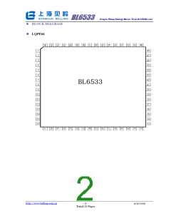
BL6533 SinglePhaseEnergyMeterICwithLCDDriver
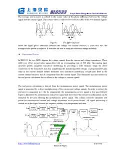
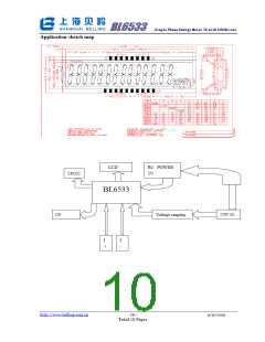
Figure 2.
Signal Processing Block Diagram
The low frequency output of the Bl6533 is generated by accumulatingm this real power information.
This low frequency inherently means a long accumulation time between output pulses. The output
frequency is therefore proportional to the average real power. This average real power information can,
in turn, be accumulated (e.g., by a counter) to generate real energy information. Because of its high
output frequency and hence shorter integration time, the CF output is proportional to the instantaneous
real power. This is useful for system calibration purposes that would take place under steady load
conditions.
ꢀ
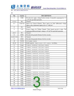
VOLTAGE CHANNEL INPUT
The output of the line voltage transducer is connected to the BL6533 at this analog input. The maximum
peak signal on Channel 2 is 330mV.
ꢀ
CURRENT CHANNEL INPUT
The voltage outputs from the current transducers are connected to the BL6533 here. The maximum
differential voltage on Current Channel 2 is ±660mV. The maximum common-mode voltage is ±
100mV.
ꢀ
Power Supply Monitor
The BL6533 contains an on-chip power supply monitor. If the supply is less than 4V±5% then the
BL6533 will go in an inactive state, i.e. no energy will be accumulated when the supply voltage is below
4V. This is useful to ensure correct device operation at power up and during power down. The power
supply monitor has built-in hysteresis and filtering. This gives a high degree of immunity to false
triggering due to noisy supplies.
The trigger level is nominally set at 4V, and the tolerance on this trigger level is about ±5%. The power
supply and decoupling for the part should be such that the ripple at VDD does not exceed 5V±5% as
specified for normal operation.
http://www.belling.com.cn
- 8 -
9/9/2009
Total 10 Pages

 BELLING [ BELLING ]