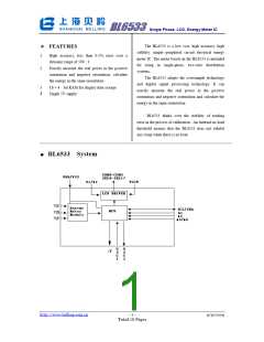
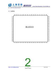
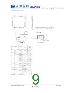
BL6533 SinglePhaseEnergyMeterICwithLCDDriver
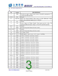
ꢀ PIN DESCRIPTIONS
ꢀ
Pin
Symbol
DESCRIPTIONS
1
VDD
Provides the supply voltage for the circuitry. It should be maintained at 5 V
±5% for specified operation.
2,3,4,5
6,7
NC
Unused
V1P,V1N
Inputs for Current Channel. These inputs are fully differential voltage
inputs with a maximum signal level of ±660 mV
Unused
8
9
NC
V2P
Positive Inputs for Voltage Channel. These inputs provide a input. The
maximum differential input voltage is 330 mV for specified operation.
Unused
10,11
NC
GND
NC
12
13,14,15,16
17
Provides the ground reference for the circuitry.
Unused
GND
VLCD
V1,V2
Com0
Com1
Com2
Com3
Seg17
Seg16
Seg15
Seg14
Seg13
Seg12
Seg11
Seg10
NC
Provides the ground reference for the circuitry.
LCD power source
18
Earth capacity,Ameliorate LCD output waveform
Common terminal driving output
Common terminal driving output
Common terminal driving output
Common terminal driving output
Segment terminal driving output
Segment terminal driving output
Segment terminal driving output
Segment terminal driving output
Segment terminal driving output
Segment terminal driving output
Segment terminal driving output
Segment terminal driving output
19,20
21
22
23
24
25
26
27
28
29
30
31
32
33,34
35
Unused
Segment terminal driving output
Segment terminal driving output
Segment terminal driving output
Segment terminal driving output
Segment terminal driving output
Segment terminal driving output
Segment terminal driving output
Seg9
36
Seg8
37
Seg7
38
Seg6
39
Seg5
40
Seg4
41
Seg3
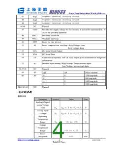
http://www.belling.com.cn
- 3 -
9/9/2009
Total 10 Pages

 BELLING [ BELLING ]