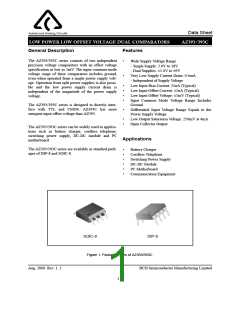
Data Sheet
LOW POWER LOW OFFSET VOLTAGE DUAL COMPARATORS
AZ393/393C
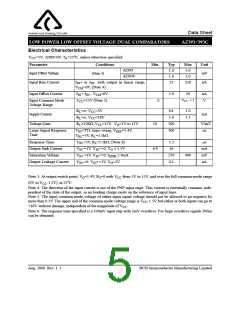
Electrical Characteristics
o
V
=5V, GND=0V, T =25 C, unless otherwise specified.
CC
A
Parameter
Conditions
(Note 3)
Min
Typ
1.0
1.0
25
Max
5.0
Unit
mV
nA
AZ393
Input Offset Voltage
Input Bias Current
AZ393C
2.0
I + or I - with output in linear range,
250
IN
IN
V
=0V, (Note 4)
CM
Input Offset Current
I +-I -, V =0V
5.0
50
nA
V
IN
IN
CM
VCC - 1.5
Input Common Mode
Voltage Range
V
=15V (Note 5)
0
CC
R =∞, V =5V
0.4
1.0
2.5
L
CC
Supply Current
mA
R =∞, V =18V
1.0
200
300
L
CC
Voltage Gain
R ≥15KΩ, V =15V, V =1V to 11V
50
V/mV
ns
L
CC
O
Large Signal Response
Time
V =TTL logic swing, V =1.4V,
IN
REF
V
=5V, R =5.1kΩ
L
RL
Response Time
V
=5V, R =5.1kΩ, (Note 6)
1.3
16
µs
RL
L
Output Sink Current
Saturation Voltage
Output Leakage Current
V -=1V, V +=0, V ≤ 1.5V
6.0
mA
mV
nA
IN
IN
O
V -=1V, V +=0, I
≤ 4mA
250
0.1
400
IN
IN
SINK
V -=0, V +=1V, V =5V
IN
IN
O
Note 3: At output switch point, V =1.4V, R =0 with V from 5V to 15V, and over the full common-mode range
O
S
CC
o
(0V to V -1.5V), at 25 C.
CC
Note 4: The direction of the input current is out of the PNP input stage. This current is essentially constant, inde-
pendent of the state of the output, so no loading charge exists on the reference of input lines.
Note 5: The input common-mode voltage of either input signal voltage should not be allowed to go negative by
more than 0.3V. The upper end of the common-mode voltage range is V -1.5V, but either or both inputs can go to
CC
+18V without damage, independent of the magnitude of V
.
CC
Note 6: The response time specified is a 100mV input step with 5mV overdrive. For large overdrive signals 300ns
can be obtained.
Aug. 2006 Rev. 1. 2
BCD Semiconductor Manufacturing Limited
5

 BCDSEMI [ BCD SEMICONDUCTOR MANUFACTURING LIMITED ]