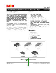
Data Sheet
LOW POWER LOW OFFSET VOLTAGE DUAL COMPARATORS
AS393/393A
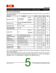
Electrical Characteristics
Limits in standard typeface are for TA=25oC, bold typeface applies over TA=-40oC to 85oC (Note 3), VCC=5V, GND=0V,
unless otherwise specified.
Parameter
Conditions
Min
Typ
Max
5.0
7
Unit
AS393
1.0
VO=1.4V, RS=0Ω,
VCC=5V to 30V
Input Offset Voltage
mV
AS393A
1.0
25
3.0
5
250
400
50
IIN+ or IIN- with output in Linear Range,
VCM=0V
Input Bias Current
Input Offset Current
nA
5.0
I
IN+-IIN -, VCM=0V
CC=30V
nA
V
200
Input Common Mode
Voltage Range (Note 4)
V
VCC -1.5
0
V
CC=5V
0.6
0.7
1.0
2
RL=∞
Supply Current
mA
VCC=30V
1.7
3
VCC=15V, RL≥15kΩ, VO=1V to 11V
Voltage Gain
50
200
200
V/mV
ns
Large Signal Response
Time
VIN =TTL Logic Swing, VREF=1.4V,
VRL=5V, RL=5.1k
VRL=5V, RL=5.1K
Response Time
1.3
16
μs
mA
nA
μA
VIN-=1V, VIN+=0, VO=1.5V
VIN-=0V, VIN+=1V, VO=5V
VIN-=0V, VIN+=1V, VO=30V
Output Sink Current
6.0
0.1
Output LeackageCurrent
Saturation Voltage
1
200
400
500
VIN-=1V, VIN+=0, ISINK≤4mA
mV
Thermal Resistance
(Junction to Case)
DIP-8
93
oC/W
SOIC-8
138
o
o
Note 3: These specifications are limited to -40 C≤ T ≤85 C. Limits over temperature are guaranteed by design,
A
but not tested in production.
Note 4: The input common-mode voltage of either input signal voltage should not be allowed to go negatively by
o
o
more than 0.3V (at 25 C). The upper end of the common-mode voltage range is V -1.5V (at 25 C), but either or
CC
both inputs can go to +36V without damages, independent of the magnitude of the V
.
CC
BCD Semiconductor Manufacturing Limited
Jan. 2013 Rev. 2. 3
5

 BCDSEMI [ BCD SEMICONDUCTOR MANUFACTURING LIMITED ]