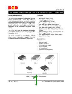
Data Sheet
LOW POWER LOW OFFSET VOLTAGE DUAL COMPARATORS
AS393/393A
Absolute Maximum Ratings (Note 1)
Parameter
Symbol
Value
40
Unit
V
VCC
Supply Voltage
VID
VIN
IIN
Differential Input Voltage
Input Voltage
40
V
-0.3 to 40
50
V
Input Current (VIN < -0.3V) (Note 2)
Output Short-Circuit Current to Ground
mA
Continuous
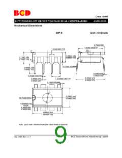
DIP-8
780
660
570
450
SOIC-8
TSSOP-8
MSOP-8
Power Dissipation (TA=25oC)
PD
mW
oC
oC
oC
TJ
Operating Junction Temperature
Storage Temperature
150
-65 to 150
260
TSTG
TLEAD
Lead Temperature (Soldering, 10 sec)
Note 1: Stresses greater than those listed under "Absolute Maximum Ratings" may cause permanent damage to the
device. These are stress ratings only, and functional operation of the device at these or any other conditions
beyond those indicated under "Recommended Operating Conditions" is not implied. Exposure to "Absolute Max-
imum Ratings" for extended periods may affect device reliability.
Note 2: This input current will only exist when the voltage at any of the input leads is driven negative. It is due to
the collector-base junction of the input PNP transistors becoming forward biased and thereby acting as input diode
clamps. In addition to this diode action, there is also lateral NPN parasitic transistor action on the IC chip. This
transistor action can cause the output voltages of the comparators to go to the V+ voltage level (or to ground for a
large overdrive) for the time duration that an input is driven negative. This is not destructive and normal output
states will re-establish when the input voltage, which was negative, again returns to a value greater than -0.3 V
DC
o
(at 25 C).
Recommended Operating Conditions
Parameter
Symbol
Min
2
Max
36
Unit
Supply Voltage
V
V
CC
o
Operating Temperature Range
T
-40
85
A
C
BCD Semiconductor Manufacturing Limited
Jan. 2013 Rev. 2. 3
4

 BCDSEMI [ BCD SEMICONDUCTOR MANUFACTURING LIMITED ]