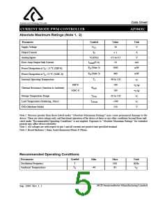
Data Sheet
CURRENT MODE PWM CONTROLLER
AP384XC
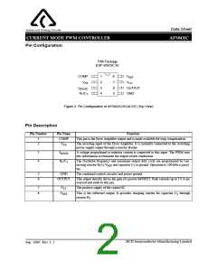
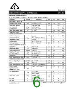
Pin Configuration
P/M Package
(DIP-8/SOIC-8)
COMP
1
8
VREF
VFB
ISENSE
RT/CT
2
3
4
7
6
5
VCC
OUTPUT
GND
Figure 2. Pin Configuration of AP3842C/3C/4C/5C (Top View)
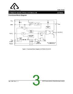
Pin Description
Pin Number
Pin Name
Function
1
2
COMP
VFB
This pin is the Error Amplifier output and is made available for loop compensation.
The inverting input of the Error Amplifier. It is normally connected to the switching
power supply output through a resistor divider.
3
4
ISENSE
RT/CT
A voltage proportional to inductor current is connected to this input. The PWM uses
this information to terminate the output switch conduction.
The Oscillator frequency and maximum output duty cycle are programmed by con-
necting resistor RT to VREF and capacitor CT to ground. Operation to 500 kHz is possi-
ble.
5
6
GND
The combined control circuitry and power ground.
OUTPUT
This output directly drives the gate of a power MOSFET. Peak currents up to 1.0 A are
sourced and sunk by this pin.
7
8
VCC
The positive supply of the control IC.
VREF
This is the reference output. It provides charging current for capacitor CT through
resistor RT.
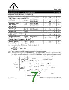
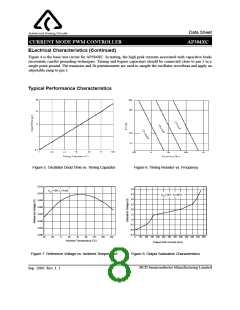
BCD Semiconductor Manufacturing Limited
Sep. 2006 Rev. 1. 1
2

 BCDSEMI [ BCD SEMICONDUCTOR MANUFACTURING LIMITED ]