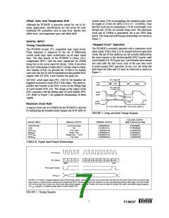
desired. Use of the MSB adjustments will only affect larger
dynamic signals (between 0dB and –6dB). This improve-
ment comes from bettering the gain match between the
upper and lower DACs at these signal levels. The change is
realized by small adjustments in the bit-2 weights of each
DAC. Great care should be taken, however, as improper
adjustment will easily result in degraded performance.
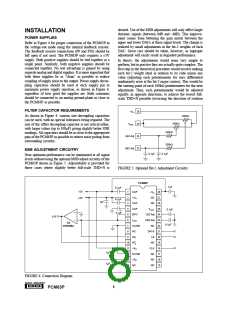
INSTALLATION
POWER SUPPLIES
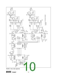
Refer to Figure 4 for proper connection of the PCM63P in
the voltage-out mode using the internal feedback resistor.
The feedback resistor connections (P9 and P10) should be
left open if not used. The PCM63P only requires a ±5V
supply. Both positive supplies should be tied together at a
single point. Similarly, both negative supplies should be
connected together. No real advantage is gained by using
separate analog and digital supplies. It is more important that
both these supplies be as “clean” as possible to reduce
coupling of supply noise to the output. Power supply decou-
pling capacitors should be used at each supply pin to
maximize power supply rejection, as shown in Figure 4,
regardless of how good the supplies are. Both commons
should be connected to an analog ground plane as close to
the PCM63P as possible.
In theory, the adjustments would seem very simple to
perform, but in practice they are actually quite complex. The
first step in the theoretical procedure would involve making
each bit-2 weight ideal in relation to its code minus one
value (adjusting each potentiometer for zero differential
nonlinearity error at the bit-2 major carries). This would be
the starting point of each 100kΩ potentiometer for the next
adjustment. Then, each potentiometer would be adjusted
equally, in opposite directions, to achieve the lowest full-
scale THD+N possible (reversing the direction of rotation
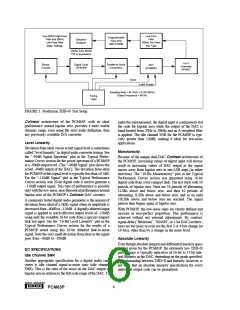
FILTER CAPACITOR REQUIREMENTS
–VA 28
As shown in Figure 4, various size decoupling capacitors
can be used, with no special tolerances being required. The
size of the offset decoupling capacitor is not critical either,
with larger values (up to 100µF) giving slightly better SNR
readings. All capacitors should be as close to the appropriate
pins of the PCM63P as possible to reduce noise pickup from
surrounding circuitry.
100kΩ
100kΩ
VPOT 25
LB2 Adj 24
UB2 Adj 23
330kΩ
330kΩ
MSB ADJUSTMENT CIRCUITRY
0.1µF
0.1µF
Near optimum performance can be maintained at all signal
levels without using the optional MSB adjust circuitry of the
PCM63P shown in Figure 5. Adjustability is provided for
those cases where slightly better full-scale THD+N is
FIGURE 5. Optional Bit-2 Adjustment Circuitry.
PCM63P
1µF
0.1µF
0.1µF
–5V
1
2
3
4
5
6
7
8
9
CAP
+VA
–VA 28
NC 27
+5V
1µF
CAP
CAP
BPO
IOUT
NC 26
VPOT 25
LB2 Adj 24
UB2 Adj 23
NC 22
0.1µF
0.1µF
+
4.7µF
±3V
1/2
OPA2604
ACOM
NC
DATA 21
LE 20
RF
1
10 RF
NC 19
2
11 –VD
12 DCOM
13 +VD
14 NC
CLK 18
NC 17
1µF
1µF
NC 16
NC 15
FIGURE 4. Connection Diagram.
®
8
PCM63P

 BB [ BURR-BROWN CORPORATION ]