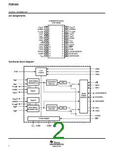
PCM1804
SLES022A – DECEMBER 2001
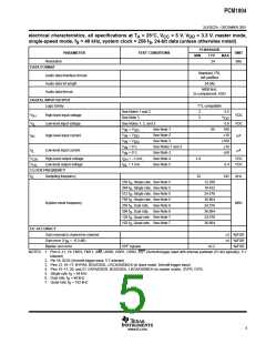
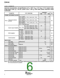
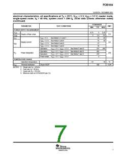
electrical characteristics, all specifications at T = 25°C, V
= 5 V, V = 3.3 V, master mode,
DD
A
CC
single-speed mode, f = 48 kHz, system clock = 256 f , 24-bit data (unless otherwise noted)
S
S
PCM1804DB
PARAMETER
TEST CONDITIONS
UNIT
MIN
TYP
MAX
Resolution
DATA FORMAT
24
Bits
2
Standard, I S,
left justified
Audio data interface format
Audio data bit length
Audio data format
24-bits
MSB first,
2s complement, DSD
DIGITAL INPUT/OUTPUT
Logic family
TTL compatible
See Notes 1 and 2
2
2
5.5
V
V
High-level input voltage
Low-level input voltage
VDC
VDC
IH
See Note 3
V
DD
0.8
See Notes 1, 2, and 3
IL
V
V
V
V
V
= V
= V
= V
,
,
,
See Note 1
See Note 2
See Note 3
See Notes 1 and 2
See Note 3
See Note 4
See Note 5
65
100
±10
IN
DD
DD
DD
I
High-level input current
µA
IN
IH
±100
±10
IN
= 0 V,
= 0 V,
IN
I
IL
Low-level input current
µA
±50
IN
V
V
High-level output voltage
Low-level output voltage
I
I
= –1 mA,
2.4
32
VDC
VDC
OH
OH
= 1 mA,
0.4
OL
OL
CLOCK FREQUENCY
f
S
Sampling frequency
192
kHz
256 f , Single rate, See Note 5
12.288
18.432
24.576
36.864
24.576
36.864
24.576
36.864
S
384 f , Single rate, See Note 5
S
512 f , Single rate, See Note 5
S
768 f , Single rate, See Note 5
S
System clock frequency
MHz
256 f , Dual rate, See Note 6
S
384 f , Dual rate, See Note 6
S
128 f , Quad rate, See Note 7
S
192 f , Quad rate, See Note 7
S
DC ACCURACY
Gain mismatch channel-to-channel
±3 %/FSR
±4 %/FSR
%/FSR
Gain error (V = –0.5 dB)
IN
Bipolar zero error
HPF bypass
±0.2
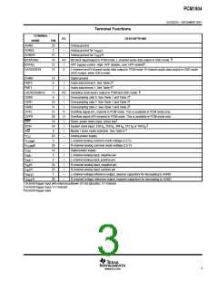
NOTES: 1. Pins 6–11, 19: FMT0, FMT1, S/M, OSR0, OSR1, OSR2, RST (Schmitt-trigger input with internal pulldown (51 kΩ typically), 5 V
tolerant)
2. Pin 18: SCKI (Schmitt-trigger input, 5 V tolerant)
3. Pins 12, 16–17: BYPAS, BCK/DSDL, LRCK/DSDBCK (in slave mode, Schmitt-trigger input)
4. Pins 15–17, 20, and 21: DATA/DSDR, BCK/DSDL, LRCK/DSDBCK (in master mode), OVFR, OVFL
5. Single rate, f = 48 kHz
S
6. Dual rate, f = 96 kHz
S
7. Quad rate, f = 192 kHz
S
5
www.ti.com

 BB [ BURR-BROWN CORPORATION ]