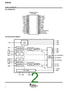
PCM1804
SLES022A – DECEMBER 2001
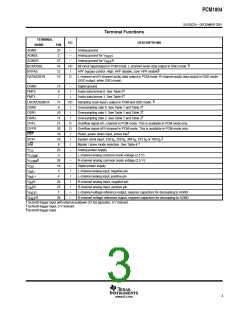
Terminal Functions
TERMINAL
NAME
AGND
I/O
DESCRIPTIONS
PIN
23
2
–
–
Analog ground
AGNDL
Analog ground for V
Analog ground for V
L
REF
AGNDR
27
16
12
15
–
R
REF
§
Bit clock input/output in PCM mode. L-channel audio data output in DSD mode.
BCK/DSDL
BYPAS
I/O
I
§
HPF bypass control. High: HPF disable, Low: HPF enable
DATA/DSDR
O
L-channel and R-channel audio data output in PCM mode. R-channel audio data output in DSD mode.
(DSD output, when DSD mode)
DGND
FMT0
13
6
–
I
Digital ground
†
†
Audio data format 0. See Table 5
Audio data format 1. See Table 5
FMT1
7
I
§
Sampling clock input / output in PCM and DSD mode.
LRCK/DSDBCK
OSR0
OSR1
OSR2
OVFL
17
9
I/O
I
†
†
†
Oversampling ratio 0. See Table 1 and Table 2
Oversampling ratio 1. See Table 1 and Table 2
Oversampling ratio 2. See Table 1 and Table 2
10
11
21
20
19
18
8
I
I
O
O
I
Overflow signal of L-channel in PCM mode. This is available in PCM mode only.
Overflow signal of R-channel in PCM mode. This is available in PCM mode only.
OVFR
RST
†
Reset, power down input, active low
‡
SCKI
I
System clock input; 128 f , 256 f , 384 f , 512 f or 768 f .
S
S
S
S
S
†
S/M
I
Master / slave mode selection. See Table 4.
Analog power supply
V
V
V
V
V
V
V
V
V
V
22
3
–
–
–
–
I
CC
L
L-channel analog common mode voltage (2.5 V)
COM
COM
DD
R
26
14
5
R-channel analog common mode voltage (2.5 V)
Digital power supply
L–
L+
R–
R+
L-channel analog input, negative pin
L-channel analog input, positive pin
R-channel analog input, negative pin
R-channel analog input, positive pin
IN
IN
IN
IN
4
I
24
25
1
I
I
L
–
–
L-channel voltage reference output, requires capacitors for decoupling to AGND
R-channel voltage reference output, requires capacitors for decoupling to AGND
REF
R
28
REF
†
‡
§
Schmitt-trigger input with internal pulldown (51 kΩ typically), 5-V tolerant.
Schmitt-trigger input, 5-V tolerant.
Schmitt-trigger input
3
www.ti.com

 BB [ BURR-BROWN CORPORATION ]