SPECIFICATIONS: VS = ±2.25V to ±18V
Boldface limits apply over the specified temperature range, TA = –40°C to +85°C
At TCASE = +25°C, VS = ±30V, Ref = 0V, and E/S pin open, unless otherwise noted.
OPA549T
PARAMETER
CONDITION
MIN
TYP
MAX
UNITS
OFFSET VOLTAGE
Input Offset Voltage
vs Temperature
VOS
VCM = 0V, IO = 0
TCASE = –40°C to +85°C
VS = ±4V to ±30V, Ref = V –
±1
±20
25
±5
mV
µV/°C
µV/V
dVOS/dT
PSRR
vs Power Supply
100
INPUT BIAS CURRENT(1)
Input Bias Current(2)
vs Temperature
IB
VCM = 0V
TCASE = –40°C to +85°C
VCM = 0V
–100
±0.5
±5
–500
nA
nA/°C
nA
Input Offset Current
IOS
±50
NOISE
Input Voltage Noise Density
Current Noise Density
en
in
f = 1kHz
f = 1kHz
70
1
nV/√Hz
pA/√Hz
INPUT VOLTAGE RANGE
Common-Mode Voltage Range: Positive
VCM
Linear Operation
Linear Operation
VCM = (V–) – 0.1V to (V+) – 3V
(V+) – 3
(V–) – 0.1
80
(V+) – 2.3
(V–) – 0.2
95
V
V
dB
Negative VCM
CMRR
Common-Mode Rejection Ratio
INPUT IMPEDANCE
Differential
Common-Mode
107 || 6
109 || 4
Ω || pF
Ω || pF
OPEN-LOOP GAIN
Open-Loop Voltage Gain
AOL
VO = ±25V, RL = 1kΩ
100
110
100
dB
dB
VO = ±25V, RL = 4Ω
FREQUENCY RESPONSE
Gain Bandwidth Product
Slew Rate
GBW
SR
0.9
9
MHz
V/µs
G = 1, 50Vp-p Step, RL = 4Ω
Full Power Bandwidth
Settling Time: ±0.1%
Total Harmonic Distortion + Noise(3)
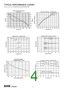
See Typical Curve
G = –10, 50V Step
f = 1kHz,RL = 4Ω,G = +3, Power = 25W
20
0.015
µs
%
THD+N
OUTPUT
Voltage Output, Positive
Negative
Positive
Negative
Negative
Maximum Continuous Current Output: dc(4)
ac(4)
IO = 2A
IO = –2A
IO = 8A
IO = –8A
RL = 8Ω to V–
(V+) – 3.2
(V–) + 1.7
(V+) – 4.8
(V–) + 4.6
(V–) + 0.3
±8
(V+) – 2.7
(V–) + 1.4
(V+) – 4.3
(V–) + 3.9
(V–) + 0.1
V
V
V
V
V
A
Arms
Waveform Cannot Exceed 10A peak
8
Output Current Limit
Current Limit Range
0 to ±10
A
A
mA
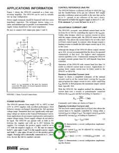
Current Limit Equation
Current Limit Tolerance(1)
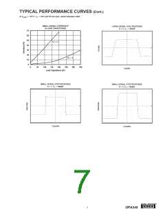
Capacitive Load Drive (Stable Operation) CLOAD
Output Disabled
ILIM = 15800 • 4.75V/(7500Ω + RCL
±200
)
RCL = 7.5kΩ (ILIM = ±5A), RL = 4Ω
±500
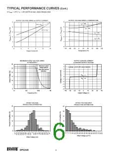
See Typical Curve
Leakage Current
Output Capacitance
Output Disabled
Output Disabled
See Typical Curve
750
pF
OUTPUT ENABLE /STATUS (E/S) PIN
Shutdown Input Mode
VE/S High (output enabled)
VE/S Low (output disabled)
IE/S High (output enabled)
IE/S Low (output disabled)
Output Disable Time
Output Enable Time
Thermal Shutdown Status Output
Normal Operation
E/S Pin Open or Forced High
E/S Pin Forced Low
(Ref) + 2.4
(Ref) + 2.4
V
V
µA
µA
µs
µs
(Ref) + 0.8
E/S Pin Indicates High
E/S Pin Indicates Low
–50
–55
1
3
Sourcing 20µA
Sinking 5µA, TJ > 160°C
(Ref) + 3.5
(Ref) + 0.2
+160
V
V
°C
°C
Thermally Shutdown
Junction Temperature, Shutdown
Reset from Shutdown
(Ref) + 0.8
(V+) – 8
+140
Ref (Reference Pin for Control Signals)
Voltage Range
Current(2)
V–
8
V
mA
–3.5
POWER SUPPLY
Specified Voltage
Operating Voltage Range, (V+) – (V–)
Quiescent Current
Quiescent Current in Shutdown Mode
VS
IQ
±30
V
V
mA
mA
60
±35
ILIM Connected to Ref IO = 0
ILIM Connected to Ref
±26
±6
TEMPERATURE RANGE
Specified Range
Operating Range
–40
–40
–55
+85
+125
+125
°C
°C
°C
Storage Range
Thermal Resistance, θJC
Thermal Resistance, θJA
1.4
30
°C/W
°C/W
No Heat Sink
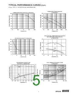
NOTES: (1) High-speed test at TJ = +25°C. (2) Positive conventional current is defined as flowing into the terminal. (3) See “Total Harmonic Distortion + Noise vs
Frequency” in the Typical Performance Curves section for additional power levels. (4) See “Safe Operating Area” (SOA) in the Typical Performance Curves section.
®
OPA549
2

 BB [ BURR-BROWN CORPORATION ]