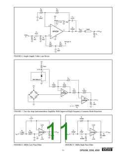
OPA350 series op amps are laser-trimmed to reduce offset
voltage difference between the N-channel and
P-channel input stages, resulting in improved common-
mode rejection and a smooth transition between the
N-channel pair and the P-channel pair. However, within the
400mV transition region PSRR, CMRR, offset voltage,
offset drift, and THD may be degraded compared to opera-
tion outside this region.
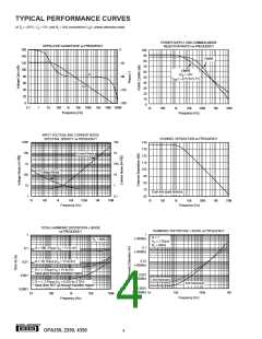
performance curve “Small-Signal Overshoot vs Capacitive
Load” shows performance with a 1kΩ resistive load. In-
creasing load resistance improves capacitive load drive ca-
pability.
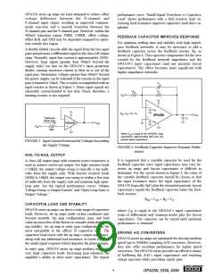
FEEDBACK CAPACITOR IMPROVES RESPONSE
For optimum settling time and stability with high-imped-
ance feedback networks, it may be necessary to add a
feedback capacitor across the feedback resistor, RF, as
shown in Figure 4. This capacitor compensates for the zero
created by the feedback network impedance and the
OPA350’s input capacitance (and any parasitic layout
capacitance). The effect becomes more significant with
higher impedance networks.
A double-folded cascode adds the signal from the two input
pairs and presents a differential signal to the class AB output
stage. Normally, input bias current is approximately 500fA.
However, large inputs (greater than 300mV beyond the
supply rails) can turn on the OPA350’s input protection
diodes, causing excessive current to flow in or out of the
input pins. Momentary voltages greater than 300mV beyond
the power supply can be tolerated if the current on the input
pins is limited to 10mA. This is easily accomplished with an
input resistor as shown in Figure 3. Many input signals are
inherently current-limited to less than 10mA, therefore, a
limiting resistor is not required.
CF
RIN
RF
V+
VIN
CIN
V+
RIN • CIN = RF • CF
VOUT
OPA350
IOVERLOAD
CL
10mA max
CIN
VOUT
OPAx350
VIN
5kΩ
Where CIN is equal to the OPA350’s input
capacitance (approximately 9pF) plus any
parastic layout capacitance.
FIGURE 3. Input Current Protection for Voltages Exceeding
the Supply Voltage.
FIGURE 4. Feedback Capacitor Improves Dynamic Perfor-
mance.
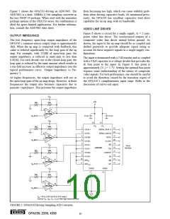
RAIL-TO-RAIL OUTPUT
It is suggested that a variable capacitor be used for the
feedback capacitor since input capacitance may vary be-
tween op amps and layout capacitance is difficult to
determine. For the circuit shown in Figure 4, the value of
the variable feedback capacitor should be chosen so that
the input resistance times the input capacitance of the
OPA350 (typically 9pF) plus the estimated parasitic layout
capacitance equals the feedback capacitor times the feed-
back resistor:
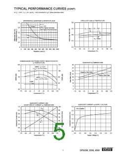
A class AB output stage with common-source transistors is
used to achieve rail-to-rail output. For light resistive loads
(>10kΩ), the output voltage swing is typically a ten milli-
volts from the supply rails. With heavier resistive loads
(600Ω to 10kΩ), the output can swing to within a few tens
of millivolts from the supply rails and maintain high open-
loop gain. See the typical performance curves “Output
Voltage Swing vs Output Current” and “Open-Loop Gain vs
Output Voltage.”
RIN • CIN = RF • CF
CAPACITIVE LOAD AND STABILITY
OPA350 series op amps can drive a wide range of capacitive
loads. However, all op amps under certain conditions may
become unstable. Op amp configuration, gain, and load
value are just a few of the factors to consider when determin-
ing stability. An op amp in unity gain configuration is the
most susceptible to the effects of capacitive load. The
capacitive load reacts with the op amp’s output impedance,
along with any additional load resistance, to create a pole in
the small-signal response which degrades the phase margin.
where CIN is equal to the OPA350’s input capacitance
(sum of differential and common-mode) plus the layout
capacitance. The capacitor can be varied until optimum
performance is obtained.
DRIVING A/D CONVERTERS
OPA350 series op amps are optimized for driving medium
speed (up to 500kHz) sampling A/D converters. However,
they also offer excellent performance for higher speed
converters. The OPA350 series provides an effective means
of buffering the A/D’s input capacitance and resulting
charge injection while providing signal gain.
In unity gain, OPA350 series op amps perform well with
very large capacitive loads. Increasing gain enhances the
amplifier’s ability to drive more capacitance. The typical
®
9
OPA350, 2350, 4350

 BB [ BURR-BROWN CORPORATION ]