Figure 5 shows the OPA350 driving an ADS7861. The
ADS7861 is a dual, 500kHz 12-bit sampling converter in
the tiny SSOP-24 package. When used with the miniature
package options of the OPA350 series, the combination is
ideal for space-limited applications. For further informa-
tion, consult the ADS7861 data sheet.
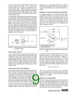
from becoming too high, which can cause stability prob-
lems when driving capacitive loads. As mentioned previ-
ously, the OPA350 has excellent capacitive load drive
capability for an op amp with its bandwidth.
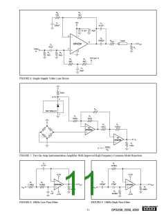
VIDEO LINE DRIVER
Figure 6 shows a circuit for a single supply, G = 2 com-
posite video line driver. The synchronized outputs of a
composite video line driver extend below ground. As
shown, the input to the op amp should be ac-coupled and
shifted positively to provide adequate signal swing to
account for these negative signals in a single-supply con-
figuration.
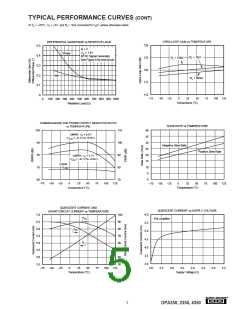
OUTPUT IMPEDANCE
The low frequency open-loop output impedance of the
OPA350’s common-source output stage is approximately
1kΩ. When the op amp is connected with feedback, this
value is reduced significantly by the loop gain of the op
amp. For example, with 122dB of open-loop gain, the
output impedance is reduced in unity-gain to less than
0.001Ω. For each decade rise in the closed-loop gain, the
loop gain is reduced by the same amount which results in
a ten-fold increase in effective output impedance (see the
typical performance curve, “Output Impedance vs Fre-
quency”).
The input is terminated with a 75Ω resistor and ac-coupled
with a 47µF capacitor to a voltage divider that provides the
dc bias point to the input. In Figure 6, this point is
approximately (V–) + 1.7V. Setting the optimal bias point
requires some understanding of the nature of composite
video signals. For best performance, one should be careful
to avoid the distortion caused by the transition region of
the OPA350’s complementary input stage. Refer to the
discussion of rail-to-rail input.
At higher frequencies, the output impedance will rise as
the open-loop gain of the op amp drops. However, at these
frequencies the output also becomes capacitive due to
parasitic capacitance. This prevents the output impedance
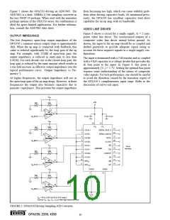
CB1
+5V
2kΩ
2kΩ
2
3
4
1/4
1
7
8
OPA4350
VIN B1
0.1µF
0.1µF
CB0
24
+VD
13
+VA
2kΩ
2kΩ
2
3
23
22
21
20
19
18
17
16
15
14
CH B1+
CH B1–
CH B0+
CH B0–
CH A1+
CH A1–
CH A0+
CH A0–
REFIN
SERIAL DATA A
SERIAL DATA B
BUSY
6
1/4
4
OPA4350
5
5
VIN B0
CLOCK
6
CA1
CS
Serial
Interface
7
ADS7861
RD
CONVST
A0
2kΩ
2kΩ
8
9
9
10
11
1/4
M0
OPA4350
10
VIN A1
REFOUT
M1
CA0
DGND
1
AGND
12
2kΩ
2kΩ
12
13
14
1/4
OPA4350
VIN A0
11
VIN = 0V to 2.45V for 0V to 4.9V output.
Choose CB1, CB0, CA1, CA0 to filter high frequency noise.
FIGURE 5. OPA4350 Driving Sampling A/D Converter.
®
OPA350, 2350, 4350
10

 BB [ BURR-BROWN CORPORATION ]