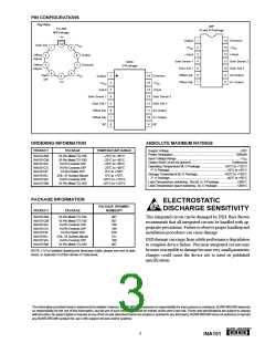
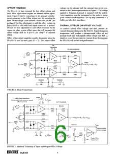
OFFSET TRIMMING
voltage can be adjusted with the optional trim circuit con-
nected to the Common pin as shown in Figure 2. The voltage
applied to Common terminal is summed with the output.
Low impedance must be maintained at this node to assure
good common-mode rejection. The op amp connected as a
buffer provides low impedance.
The INA101 is laser trimmed for low offset voltage and
drift. Most applications require no external offset adjust-
ment. Figure 2 shows connection of an optional potentio-
meter connected to the Offset Adjust pins for trimming the
input offset voltage. (Pin numbers shown are for the DIP
package.) Use this adjustment to null the offset voltage in
high gain (G ≥ 100) with both inputs connected to ground.
Do not use this adjustment to null offset produced by the
source or other system offset since this will increase the
offset voltage drift by 0.3µV/°C per 100µV of adjusted
offset.
THERMAL EFFECTS ON OFFSET VOLTAGE
To achieve lowest offset voltage and drift, prevent air
currents from circulating near the INA101. Rapid changes in
temperature will produce a thermocouple effect on the
package leads that will degrade offset voltage and drift. A
shield or cover that prevents air currents from flowing near
the INA101 will assure best performance.
Offset of the output amplifier usually dominates when the
INA101 is used in unity gain (G = 1). The output offset
No
Connection
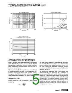
TO-100 PACKAGE
INA101
2
3
10
1
E2
A1
10kΩ
10kΩ
20kΩ
20kΩ
Output
VO = G (E1 – E2)
8
40kΩ
RG
A3
G = 1 +
RG
4
5
A2
7
E1
10kΩ
10kΩ
9
6
Tantalum
Tantalum
+
+
1µF
1µF
+15V –15V
FIGURE 1. Basic Connections.
+15V
100kΩ
Input Offset Adjustment
Do not use to null source or system
offset (see text).
A1 Output
DIP PACKAGE
INA101
6
7
3
E2
A1
10kΩ
10kΩ
4
5
20kΩ
20kΩ
RG
A3
V
O = G (E1 – E2) +VCOM
10
1
11
40kΩ
RG
G = 1 +
Common
+15V
VCOM
A2
12
E1
14
10kΩ
10kΩ
Approximately
±15mV Range
2
13
OPA177
1MΩ
Pinout shown
is for DIP packages.
+15V –15V
A2 Output
100kΩ
–15V
Output Offset
Adjustment
1kΩ
FIGURE 2. Optional Trimming of Input and Output Offset Voltage.
®
6
INA101

 BB [ BURR-BROWN CORPORATION ]