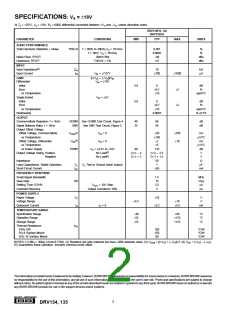
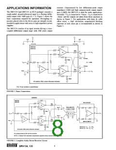
resistors. Characterized by low differential-mode output
impedance (50Ω) and high common-mode output imped-
ance (1.6kΩ), the DRV134 is ideal for audio applications.
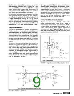
Normally, +VO is connected to +Sense, –VO is connected to
–Sense, and the outputs are taken from these junctions as
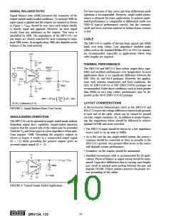
shown in Figure 1. For applications with large dc cable
offset errors, a 10µF electrolytic nonpolarized blocking
capacitor at each sense pin is recommended as shown in
Figure 2.
APPLICATIONS INFORMATION
The DRV134 (and DRV135 in SO-8 package) converts a
single-ended, ground-referenced input to a floating differ-
ential output with +6dB gain (G = 2). Figure 1 shows the
basic connections required for operation. Decoupling ca-
pacitors placed close to the device pins are strongly recom-
mended in applications with noisy or high impedance power
supplies.
The DRV134 consists of an input inverter driving a cross-
coupled differential output stage with 50Ω series output
V–
V+
1µF
1µF
5
(11)
6 (12)
DRV134
DRV135
50Ω
8
+VO
A2
(14)
7
(13)
+Sense
G = +6dB
–Sense
10kΩ
4
VIN
(6)
2
(4)
1
A1
50Ω
3
Gnd
–VO
A3
(5)
(3)
10kΩ
All resistors 30kΩ unless otherwise indicated.
SOL-16 pin numbers in parentheses.
FIGURE 1. Basic Connections.
DRIVER
DRV134
DRV135
RECEIVER
50Ω
8
7
A2
–VO
5
6
1
10µF(1)
BALANCED
CABLE PAIR
+VO
2
10kΩ
4
3
VO
VIN
10µF(1)
2
1
3
–VO
A1
50Ω
+VO
Gnd
A3
INA134, INA137
INA134 (G = 1): VO = 2VIN
INA137 (G = 1/2): VO = VIN
10kΩ
All resistors 30kΩ unless otherwise indicated.
Pin numbers shown for DIP and SO-8 versions.
NOTE: (1) Optional 10µF electrolytic (nonpolarized) capacitors reduce common-mode offset errors.
FIGURE 2. Complete Audio Driver/Receiver Circuit.
®
8
DRV134, 135

 BB [ BURR-BROWN CORPORATION ]