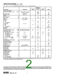
SPECIFICATIONS: VS = ±18V
At TA = +25°C, VS = ±18V, RL = 600Ω differential connected between +VO and –VO, unless otherwise noted.
DRV134PA, UA
DRV135UA
PARAMETER
CONDITIONS
MIN
TYP
MAX
UNITS
AUDIO PERFORMANCE
Total Harmonic Distortion + Noise
THD+N
f = 20Hz to 20kHz,VO = 10Vrms
f = 1kHz, VO = 10Vrms
20kHz BW
0.001
0.0005
–98
%
%
Noise Floor, RTO(1)
Headroom, RTO(1)
dBu
dBu
THD+N < 1%
+27
INPUT
Input Impedance(2)
ZIN
IIN
10
kΩ
µA
Input Current
VIN = ±7.07V
±700
±1000
GAIN
[(+VO) – (–VO)]/VIN
Differential
VIN = ±10V
Initial
5.8
5.8
6
dB
%
Error
±0.1
±10
±2
±2
vs Temperature
Single-Ended
Initial
ppm/°C
VIN = ±5V
6
dB
%
Error
±0.7
±10
vs Temperature
Nonlinearity
ppm/°C
% of FS
0.0003
OUTPUT
Common-Mode Rejection, f = 1kHz
Signal Balance Ratio, f = 1kHz
Output Offset Voltage
Offset Voltage, Common-Mode
vs Temperature
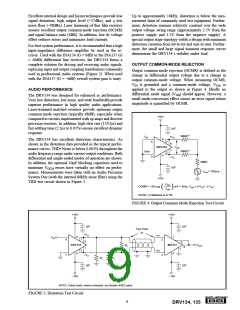
OCMR See OCMR Test Circuit, Figure 4
46
35
68
54
dB
dB
SBR
See SBR Test Circuit, Figure 5
(3)
VOCM
VIN = 0
VIN = 0
±50
±150
±1
±250
±10
mV
µV/°C
mV
µV/°C
dB
(4)
Offset Voltage, Differential
vs Temperature
VOD
±5
vs Power Supply
PSRR
VS = ±4.5V to ±18V
No Load(5)
80
110
Output Voltage Swing, Positive
Negative
(V+) – 3
(V–) + 2
(V+) – 2.5
(V–) + 1.5
50
V
No Load(5)
V
Impedance
Ω
Load Capacitance, Stable Operation
Short-Circuit Current
CL
CL Tied to Ground (each output)
1
µF
ISC
±85
mA
FREQUENCY RESPONSE
Small-Signal Bandwidth
Slew Rate
1.5
15
2.5
3
MHz
V/µs
µs
SR
Settling Time: 0.01%
Overload Recovery
VOUT = 10V Step
Output Overdriven 10%
µs
POWER SUPPLY
Rated Voltage
VS
IQ
±18
V
V
Voltage Range
Quiescent Current
±4.5
±18
IO = 0
±5.2
±5.5
mA
TEMPERATURE RANGE
Specification Range
Operation Range
–40
–55
–55
+85
+125
+125
°C
°C
°C
Storage Range
Thermal Resistance
8-Pin DIP
SO-8 Surface Mount
SOL-16 Surface Mount
θJA
100
150
80
°C/W
°C/W
°C/W
NOTES: (1) dBu = 20log (Vrms/0.7746). (2) Resistors are ratio matched but have ±20% absolute value. (3) VOCM = [(+VO) + (–VO)]/2. (4) VOD = (+VO) – (–VO).
(5) Guarantees linear operation. Includes common-mode offset.
The information provided herein is believed to be reliable; however, BURR-BROWN assumes no responsibility for inaccuracies or omissions. BURR-BROWN assumes
no responsibility for the use of this information, and all use of such information shall be entirely at the user’s own risk. Prices and specifications are subject to change
without notice. No patent rights or licenses to any of the circuits described herein are implied or granted to any third party. BURR-BROWN does not authorize or warrant
any BURR-BROWN product for use in life support devices and/or systems.
®
2
DRV134, 135

 BB [ BURR-BROWN CORPORATION ]