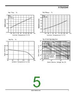
STK0260
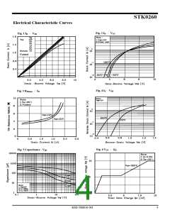
Electrical Characteristics
Characteristic
(Ta=25°C)
Min. Typ. Max. Unit
Symbol
BVDSS
VGS(th)
IDSS
Test Condition
Drain-source breakdown voltage
ID=250µA, VGS=0
600
-
-
4.0
1
V
Gate-threshold voltage
ID=250µA, VDS= VGS
VDS=600V, VGS=0V
VDS=0V, VGS=±30V
VGS=10V, ID=0.3A
VDS=10V, ID=0.3A
2.0
-
-
V
Drain-source leakage current
Gate-source leakage
-
µA
nA
Ω
IGSS
-
-
±100
4.7
-
Drain-Source on-resistance
Forward transfer admittance
Input capacitance
Output capacitance
Reverse transfer capacitance
Turn-on delay time
Rise time
④
④
RDS(ON)
gfs
-
3.8
2.3
290
33
6.0
22
10.5
7
-
S
Ciss
Coss
Crss
td(on)
tr
-
435
49
9.0
-
VGS=0V, VDS=25V, f=1MHz
pF
ns
nC
-
-
-
VDD=300V, VGS=10V
ID=0.6A, RG=25Ω
-
-
Turn-off delay time
Fall time
td(off)
tf
-
-
③④
-
10.5
8.4
1.4
2.6
-
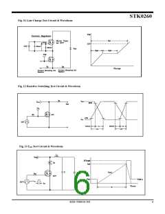
Total gate charge
Qg
-
12.6
2.1
3.9
VDD=300V, VGS=10V
ID=0.6A
Gate-source charge
Gate-drain charge
Qgs
-
③④
Qgd
-
Source-Drain Diode Ratings and Characteristics
(Ta=25°C)
Min Typ Max Unit
Characteristic
Continuous source current
Source current (Pulsed)
Forward voltage
Symbol
Test Condition
IS
ISM
VSD
trr
-
-
-
-
-
-
0.6
2.4
1.4
-
Integral reverse diode
in the MOSFET
A
①
④
-
VGS=0V, IS=0.3A
-
V
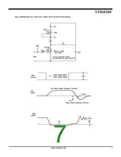
Reverse recovery time
Reverse recovery charge
230
0.84
ns
uC
Is=0.6A, VGS=0V
dis/dt=100A/us
Qrr
-
Note ;
① Repetitive Rating : Pulse Width Limited by Maximum Junction Temperature
② L=20mH, IAS=0.6A, VDD=50V, RG=25Ω
③ Pulse Test : Pulse Width< 300us, Duty cycle≤2%
④ Essentially independent of operating temperature
KSD-T0H010-001
3

 AUK [ AUK CORP ]