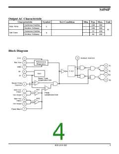
S494P
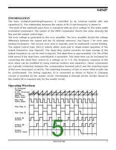
Test Circuit
Fig.1Error Amplifier Test Circuit
Fig.2 Current Limit sense Amplifier Test Circuit
1
+
+
1
+
ERROR
ERROR
3
V
3
V
VIN
AMP
AMP
-
REF
V
-
2
2
-
+
16
+
16
+
ERROR
ERROR
VIN
AMP
-
-
AMP
-
REF
V
15
15
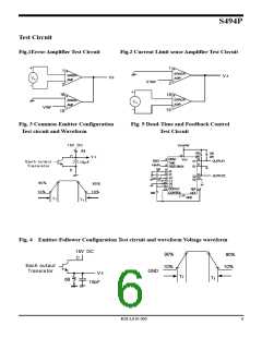
Fig. 3 Common-Emitter Configuration
Test circuit and Waveform
Fig. 5 Dead-Time and Feedback Control
Test Circuit
15V DC
68
Vcc=15V
150
150
2W
12
C
2W
8
V c
4 DEAD
Vcc
TEST
OUTPUT1
C1
Each output
15pF
TIME
3
9
Inputs
Trans is tor
FEED BACK
E1
12K
6
5
1
2
E
T
R
T
C
11
10
OUTPUT2
C2
E2
(+)
(-)
(+)
0.01uF
90%
10%
16
15
13
90%
10%
(-)
OUTPUT
REF 14
OUT
CONTROL
7
50K
GND
Tr
T
f
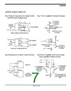
Fig. 4 Emitter-Follower Configuration Test circuit and waveform Voltage waveform
15V DC
90%
10%
90%
10%
C
Each output
Transistor
GND
E
V
Tr
T
f
68
15pF
KSI-L010-000
6

 AUK [ AUK CORP ]