AT90CAN128
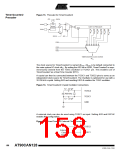
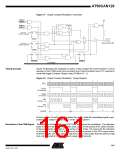
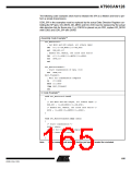
Figure 77. Output Compare Modulator, Schematic
COM0A1
COM0A0
Vcc
COM1C1
COM1C0
Modulator
0
1
(From T/C1
Waveform Generator)
D
Q
1
0
OC1C
Pin
OC0A / OC1C / PB7
(From T/C0
Waveform Generator)
D
Q
OC0A
D
Q
D
Q
PORTB7
DDRB7
DATABUS
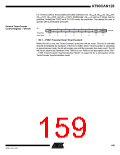
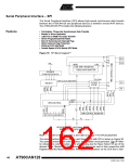
Timing Example
Figure 78 illustrates the modulator in action. In this example the Timer/Counter1 is set to
operate in fast PWM mode (non-inverted) and Timer/Counter0 uses CTC waveform
mode with toggle Compare Output mode (COMnx1:0 = 1).
Figure 78. Output Compare Modulator, Timing Diagram
clkI/O
OC1C
(FPWM Mode)
OC0A
(CTC Mode)
PB7
(PORTB7 = 0)
PB7
(PORTB7 = 1)
1
2
3
(Period)
In this example, Timer/Counter0 provides the carrier, while the modulating signal is gen-
erated by the Output Compare unit C of the Timer/Counter1.
Resolution of the PWM Signal The resolution of the PWM signal (OC1C) is reduced by the modulation. The reduction
factor is equal to the number of system clock cycles of one period of the carrier (OC0A).
In this example the resolution is reduced by a factor of two. The reason for the reduction
is illustrated in Figure 78 at the second and third period of the PB7 output when
PORTB7 equals zero. The period 2 high time is one cycle longer than the period 3 high
time, but the result on the PB7 output is equal in both periods.
161
4250E–CAN–12/04

 ATMEL [ ATMEL ]