ATtiny2313/V
128 kHz Internal
Oscillator
The 128 kHz Internal Oscillator is a low power Oscillator providing a clock of 128 kHz.
The frequency is nominal at 3 V and 25°C. This clock may be selected as the system
clock by programming the CKSEL Fuses to “0110 - 0111”.
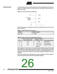
When this clock source is selected, start-up times are determined by the SUT Fuses as
shown in Table 11.
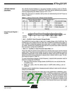
Table 11. Start-up Times for the 128 kHz Internal Oscillator
Start-up Time from Power-
down and Power-save
Additional Delay from
Reset
SUT1..0
00
Recommended Usage
BOD enabled
6 CK
6 CK
6 CK
14CK
01
14CK + 4 ms
14CK + 64 ms
Reserved
Fast rising power
Slowly rising power
10
11
Clock Prescale Register –
CLKPR
Bit
7
CLKPCE
R/W
0
6
–
5
–
4
–
3
2
1
0
CLKPS3
R/W
CLKPS2
R/W
CLKPS1
R/W
CLKPS0
R/W
CLKPR
Read/Write
Initial Value
R
0
R
0
R
0
See Bit Description
• Bit 7 – CLKPCE: Clock Prescaler Change Enable
The CLKPCE bit must be written to logic one to enable change of the CLKPS bits. The
CLKPCE bit is only updated when the other bits in CLKPR are simultaneously written to
zero. CLKPCE is cleared by hardware four cycles after it is written or when CLKPS bits
are written. Rewriting the CLKPCE bit within this time-out period does neither extend the
time-out period, nor clear the CLKPCE bit.
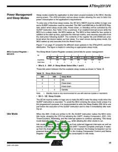
• Bits 3..0 – CLKPS3..0: Clock Prescaler Select Bits 3 - 0
These bits define the division factor between the selected clock source and the internal
system clock. These bits can be written run-time to vary the clock frequency to suit the
application requirements. As the divider divides the master clock input to the MCU, the
speed of all synchronous peripherals is reduced when a division factor is used. The divi-
sion factors are given in Table 12.
To avoid unintentional changes of clock frequency, a special write procedure must be
followed to change the CLKPS bits:
1. Write the Clock Prescaler Change Enable (CLKPCE) bit to one and all other bits
in CLKPR to zero.
2. Within four cycles, write the desired value to CLKPS while writing a zero to
CLKPCE.
Interrupts must be disabled when changing prescaler setting to make sure the write pro-
cedure is not interrupted.
The CKDIV8 Fuse determines the initial value of the CLKPS bits. If CKDIV8 is unpro-
grammed, the CLKPS bits will be reset to “0000”. If CKDIV8 is programmed, CLKPS bits
are reset to “0011”, giving a division factor of 8 at start up. This feature should be used if
the selected clock source has a higher frequency than the maximum frequency of the
device at the present operating conditions. Note that any value can be written to the
CLKPS bits regardless of the CKDIV8 Fuse setting. The Application software must
ensure that a sufficient division factor is chosen if the selected clock source has a higher
27
2543F–AVR–08/04

 ATMEL [ ATMEL ]