ATmega64A
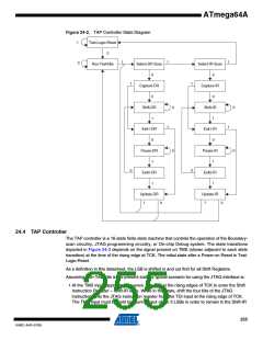
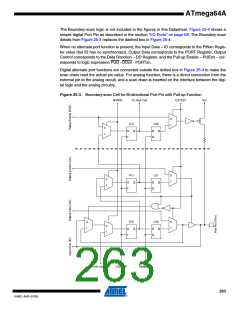
25. IEEE 1149.1 (JTAG) Boundary-scan
25.1 Features
• JTAG (IEEE std. 1149.1 Compliant) Interface
• Boundary-scan Capabilities According to the JTAG Standard
• Full Scan of all Port Functions as well as Analog Circuitry Having Off-chip Connections
• Supports the Optional IDCODE Instruction
• Additional Public AVR_RESET Instruction to Reset the AVR
25.2 Overview
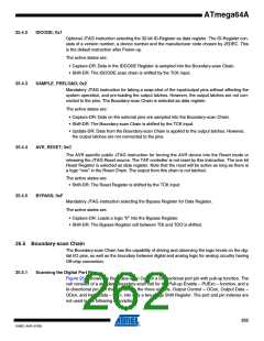
The Boundary-scan chain has the capability of driving and observing the logic levels on the digi-
tal I/O pins, as well as the boundary between digital and analog logic for analog circuitry having
Off-chip connections. At system level, all ICs having JTAG capabilities are connected serially by
the TDI/TDO signals to form a long Shift Register. An external controller sets up the devices to
drive values at their output pins, and observe the input values received from other devices. The
controller compares the received data with the expected result. In this way, Boundary-scan pro-
vides a mechanism for testing interconnections and integrity of components on Printed Circuits
Boards by using the four TAP signals only.
The four IEEE 1149.1 defined mandatory JTAG instructions IDCODE, BYPASS, SAMPLE/PRE-
LOAD, and EXTEST, as well as the AVR specific public JTAG instruction AVR_RESET can be
used for testing the printed circuit board. Initial scanning of the data register path will show the
ID-Code of the device, since IDCODE is the default JTAG instruction. It may be desirable to
have the AVR device in reset during test mode. If not reset, inputs to the device may be deter-
mined by the scan operations, and the internal software may be in an undetermined state when
exiting the test mode. Entering reset, the outputs of any Port Pin will instantly enter the high
impedance state, making the HIGHZ instruction redundant. If needed, the BYPASS instruction
can be issued to make the shortest possible scan chain through the device. The device can be
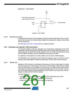
set in the reset state either by pulling the external RESET pin low, or issuing the AVR_RESET
instruction with appropriate setting of the Reset Data Register.
The EXTEST instruction is used for sampling external pins and loading output pins with data.
The data from the output latch will be driven out on the pins as soon as the EXTEST instruction
is loaded into the JTAG IR-Register. Therefore, the SAMPLE/PRELOAD should also be used for
setting initial values to the scan ring, to avoid damaging the board when issuing the EXTEST
instruction for the first time. SAMPLE/PRELOAD can also be used for taking a snapshot of the
external pins during normal operation of the part.
The JTAGEN Fuse must be programmed and the JTD bit in the I/O Register MCUCSR must be
cleared to enable the JTAG Test Access Port.
When using the JTAG interface for Boundary-scan, using a JTAG TCK clock frequency higher
than the internal chip frequency is possible. The chip clock is not required to run.
25.3 Data Registers
The data registers relevant for Boundary-scan operations are:
• Bypass Register
• Device Identification Register
• Reset Register
• Boundary-scan Chain
259
8160C–AVR–07/09

 ATMEL [ ATMEL ]