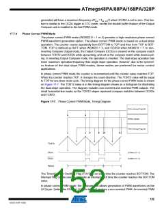
ATmega48PA/88PA/168PA/328P
• Description of wake up from Power-save or ADC Noise Reduction mode when the timer is
clocked asynchronously: When the interrupt condition is met, the wake up process is started
on the following cycle of the timer clock, that is, the timer is always advanced by at least one
before the processor can read the counter value. After wake-up, the MCU is halted for four
cycles, it executes the interrupt routine, and resumes execution from the instruction following
SLEEP.
• Reading of the TCNT2 Register shortly after wake-up from Power-save may give an incorrect
result. Since TCNT2 is clocked on the asynchronous TOSC clock, reading TCNT2 must be
done through a register synchronized to the internal I/O clock domain. Synchronization takes
place for every rising TOSC1 edge. When waking up from Power-save mode, and the I/O clock
(clkI/O) again becomes active, TCNT2 will read as the previous value (before entering sleep)
until the next rising TOSC1 edge. The phase of the TOSC clock after waking up from Power-
save mode is essentially unpredictable, as it depends on the wake-up time. The recommended
procedure for reading TCNT2 is thus as follows:
a. Write any value to either of the registers OCR2x or TCCR2x.
b. Wait for the corresponding Update Busy Flag to be cleared.
c. Read TCNT2.
During asynchronous operation, the synchronization of the Interrupt Flags for the asynchronous
timer takes 3 processor cycles plus one timer cycle. The timer is therefore advanced by at least
one before the processor can read the timer value causing the setting of the Interrupt Flag. The
Output Compare pin is changed on the timer clock and is not synchronized to the processor
clock.
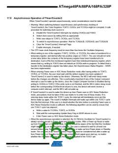
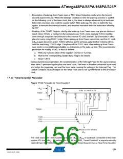
17.10 Timer/Counter Prescaler
Figure 17-12. Prescaler for Timer/Counter2
clkI/O
clkT2S
10-BIT T/C PRESCALER
Clear
TOSC1
AS2
PSRASY
0
CS20
CS21
CS22
TIMER/COUNTER2 CLOCK SOURCE
clkT2
The clock source for Timer/Counter2 is named clkT2S. clkT2S is by default connected to the main
system I/O clock clkIO. By setting the AS2 bit in ASSR, Timer/Counter2 is asynchronously
clocked from the TOSC1 pin. This enables use of Timer/Counter2 as a Real Time Counter
156
8161D–AVR–10/09

 ATMEL [ ATMEL ]