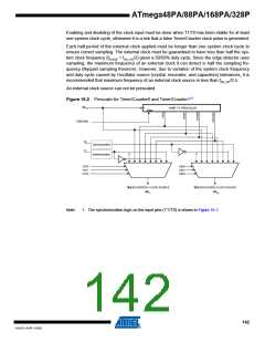
ATmega48PA/88PA/168PA/328P
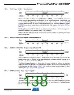
15.11.4 TCNT1H and TCNT1L – Timer/Counter1
Bit
7
6
5
4
3
2
1
0
(0x85)
TCNT1[15:8]
TCNT1[7:0]
TCNT1H
TCNT1L
(0x84)
Read/Write
Initial Value
R/W
0
R/W
0
R/W
0
R/W
R/W
0
R/W
0
R/W
0
R/W
0
0
The two Timer/Counter I/O locations (TCNT1H and TCNT1L, combined TCNT1) give direct
access, both for read and for write operations, to the Timer/Counter unit 16-bit counter. To
ensure that both the high and low bytes are read and written simultaneously when the CPU
accesses these registers, the access is performed using an 8-bit temporary High Byte Register
(TEMP). This temporary register is shared by all the other 16-bit registers. See Section “15.3” on
page 115.
Modifying the counter (TCNT1) while the counter is running introduces a risk of missing a com-
pare match between TCNT1 and one of the OCR1x Registers.
Writing to the TCNT1 Register blocks (removes) the compare match on the following timer clock
for all compare units.
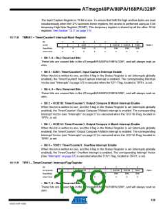
15.11.5 OCR1AH and OCR1AL – Output Compare Register 1 A
Bit
7
6
5
4
3
2
1
0
(0x89)
OCR1A[15:8]
OCR1A[7:0]
OCR1AH
OCR1AL
(0x88)
Read/Write
Initial Value
R/W
0
R/W
0
R/W
0
R/W
R/W
R/W
0
R/W
0
R/W
0
0
0
15.11.6 OCR1BH and OCR1BL – Output Compare Register 1 B
Bit
7
6
5
4
3
2
1
0
(0x8B)
OCR1B[15:8]
OCR1B[7:0]
OCR1BH
OCR1BL
(0x8A)
Read/Write
Initial Value
R/W
0
R/W
0
R/W
0
R/W
R/W
R/W
0
R/W
0
R/W
0
0
0
The Output Compare Registers contain a 16-bit value that is continuously compared with the
counter value (TCNT1). A match can be used to generate an Output Compare interrupt, or to
generate a waveform output on the OC1x pin.
The Output Compare Registers are 16-bit in size. To ensure that both the high and low bytes are
written simultaneously when the CPU writes to these registers, the access is performed using an
8-bit temporary High Byte Register (TEMP). This temporary register is shared by all the other
16-bit registers. See Section “15.3” on page 115.
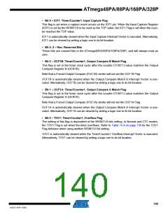
15.11.7 ICR1H and ICR1L – Input Capture Register 1
Bit
7
6
5
4
3
2
1
0
(0x87)
ICR1[15:8]
ICR1[7:0]
ICR1H
ICR1L
(0x86)
Read/Write
Initial Value
R/W
0
R/W
0
R/W
0
R/W
0
R/W
0
R/W
0
R/W
0
R/W
0
The Input Capture is updated with the counter (TCNT1) value each time an event occurs on the
ICP1 pin (or optionally on the Analog Comparator output for Timer/Counter1). The Input Capture
can be used for defining the counter TOP value.
138
8161D–AVR–10/09

 ATMEL [ ATMEL ]