ATmega48PA/88PA/168PA/328P
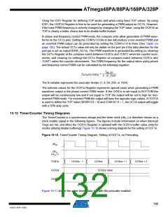
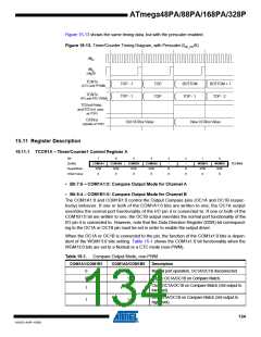
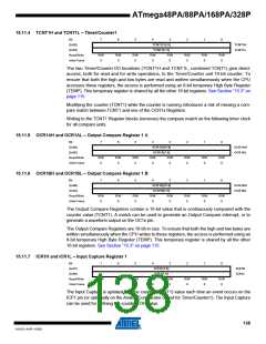
Figure 15-13 shows the same timing data, but with the prescaler enabled.
Figure 15-13. Timer/Counter Timing Diagram, with Prescaler (fclk_I/O/8)
clk
I/O
clk
Tn
(clk /8)
I/O
TCNTn
TOP - 1
TOP - 1
TOP
TOP
BOTTOM
TOP - 1
BOTTOM + 1
TOP - 2
(CTC and FPWM)
TCNTn
(PC and PFC PWM)
TOVn(FPWM)
and ICFn(if used
as TOP)
OCRnx
(Update at TOP)
Old OCRnx Value
New OCRnx Value
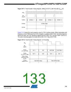
15.11 Register Description
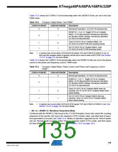
15.11.1 TCCR1A – Timer/Counter1 Control Register A
Bit
7
COM1A1
R/W
6
COM1A0
R/W
5
COM1B1
R/W
4
3
–
2
–
1
WGM11
R/W
0
0
WGM10
R/W
0
COM1B0
R/W
0
TCCR1A
(0x80)
Read/Write
Initial Value
R
0
R
0
0
0
0
• Bit 7:6 – COM1A1:0: Compare Output Mode for Channel A
• Bit 5:4 – COM1B1:0: Compare Output Mode for Channel B
The COM1A1:0 and COM1B1:0 control the Output Compare pins (OC1A and OC1B respec-
tively) behavior. If one or both of the COM1A1:0 bits are written to one, the OC1A output
overrides the normal port functionality of the I/O pin it is connected to. If one or both of the
COM1B1:0 bit are written to one, the OC1B output overrides the normal port functionality of the
I/O pin it is connected to. However, note that the Data Direction Register (DDR) bit correspond-
ing to the OC1A or OC1B pin must be set in order to enable the output driver.
When the OC1A or OC1B is connected to the pin, the function of the COM1x1:0 bits is depen-
dent of the WGM13:0 bits setting. Table 15-1 shows the COM1x1:0 bit functionality when the
WGM13:0 bits are set to a Normal or a CTC mode (non-PWM).
Table 15-1. Compare Output Mode, non-PWM
COM1A1/COM1B1
COM1A0/COM1B0
Description
0
0
0
1
Normal port operation, OC1A/OC1B disconnected.
Toggle OC1A/OC1B on Compare Match.
Clear OC1A/OC1B on Compare Match (Set output to
low level).
1
1
0
1
Set OC1A/OC1B on Compare Match (Set output to
high level).
134
8161D–AVR–10/09

 ATMEL [ ATMEL ]