ATmega48PA/88PA/168PA/328P
The PWM resolution for fast PWM can be fixed to 8-, 9-, or 10-bit, or defined by either ICR1 or
OCR1A. The minimum resolution allowed is 2-bit (ICR1 or OCR1A set to 0x0003), and the max-
imum resolution is 16-bit (ICR1 or OCR1A set to MAX). The PWM resolution in bits can be
calculated by using the following equation:
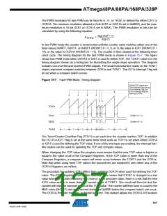
log(TOP + 1)
R
= ----------------------------------
FPWM
log(2)
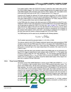
In fast PWM mode the counter is incremented until the counter value matches either one of the
fixed values 0x00FF, 0x01FF, or 0x03FF (WGM13:0 = 5, 6, or 7), the value in ICR1 (WGM13:0 =
14), or the value in OCR1A (WGM13:0 = 15). The counter is then cleared at the following timer
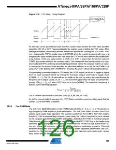
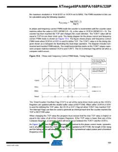
clock cycle. The timing diagram for the fast PWM mode is shown in Figure 15-7. The figure
shows fast PWM mode when OCR1A or ICR1 is used to define TOP. The TCNT1 value is in the
timing diagram shown as a histogram for illustrating the single-slope operation. The diagram
includes non-inverted and inverted PWM outputs. The small horizontal line marks on the TCNT1
slopes represent compare matches between OCR1x and TCNT1. The OC1x Interrupt Flag will
be set when a compare match occurs.
Figure 15-7. Fast PWM Mode, Timing Diagram
OCRnx/TOP Update and
TOVn Interrupt Flag Set and
OCnA Interrupt Flag Set
or ICFn Interrupt Flag Set
(Interrupt on TOP)
TCNTn
(COMnx1:0 = 2)
OCnx
(COMnx1:0 = 3)
OCnx
1
2
3
4
5
6
7
8
Period
The Timer/Counter Overflow Flag (TOV1) is set each time the counter reaches TOP. In addition
the OC1A or ICF1 Flag is set at the same timer clock cycle as TOV1 is set when either OCR1A
or ICR1 is used for defining the TOP value. If one of the interrupts are enabled, the interrupt han-
dler routine can be used for updating the TOP and compare values.
When changing the TOP value the program must ensure that the new TOP value is higher or
equal to the value of all of the Compare Registers. If the TOP value is lower than any of the
Compare Registers, a compare match will never occur between the TCNT1 and the OCR1x.
Note that when using fixed TOP values the unused bits are masked to zero when any of the
OCR1x Registers are written.
The procedure for updating ICR1 differs from updating OCR1A when used for defining the TOP
value. The ICR1 Register is not double buffered. This means that if ICR1 is changed to a low
value when the counter is running with none or a low prescaler value, there is a risk that the new
ICR1 value written is lower than the current value of TCNT1. The result will then be that the
counter will miss the compare match at the TOP value. The counter will then have to count to the
MAX value (0xFFFF) and wrap around starting at 0x0000 before the compare match can occur.
The OCR1A Register however, is double buffered. This feature allows the OCR1A I/O location
127
8161D–AVR–10/09

 ATMEL [ ATMEL ]