ATmega16/32/64/M1/C1
In phase correct PWM mode, the compare unit allows generation of PWM waveforms on the
OC0x pins. Setting the COM0x1:0 bits to two will produce a non-inverted PWM. An inverted
PWM output can be generated by setting the COM0x1:0 to three: Setting the COM0A0 bits to
one allows the OC0A pin to toggle on Compare Matches if the WGM02 bit is set. This option is
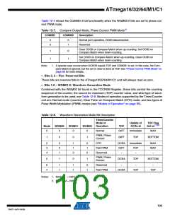
not available for the OC0B pin (see Table 12-7 on page 103). The actual OC0x value will only be
visible on the port pin if the data direction for the port pin is set as output. The PWM waveform is
generated by clearing (or setting) the OC0x Register at the compare match between OCR0x and
TCNT0 when the counter increments, and setting (or clearing) the OC0x Register at compare
match between OCR0x and TCNT0 when the counter decrements. The PWM frequency for the
output when using phase correct PWM can be calculated by the following equation:
f
clk_I/O
f
= --------------------
OCnxPCPWM
N
510
The N variable represents the prescale factor (1, 8, 64, 256, or 1024).
The extreme values for the OCR0A Register represent special cases when generating a PWM
waveform output in the phase correct PWM mode. If the OCR0A is set equal to BOTTOM, the
output will be continuously low and if set equal to MAX the output will be continuously high for
non-inverted PWM mode. For inverted PWM the output will have the opposite logic values.
At the very start of period 2 in Figure 12-7 OCnx has a transition from high to low even though
there is no Compare Match. The point of this transition is to guarantee symmetry around BOT-
TOM. There are two cases that give a transition without Compare Match.
• OCRnx changes its value from MAX, like in Figure 12-7. When the OCR0A value is MAX the
OCn pin value is the same as the result of a down-counting Compare Match. To ensure
symmetry around BOTTOM the OCnx value at MAX must correspond to the result of an
up-counting Compare Match.
• The timer starts counting from a value higher than the one in OCRnx, and for that reason
misses the Compare Match and hence the OCnx change that would have happened on the
way up.
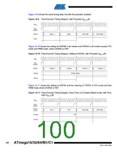
12.7 Timer/Counter Timing Diagrams
The Timer/Counter is a synchronous design and the timer clock (clkT0) is therefore shown as a
clock enable signal in the following figures. The figures include information on when interrupt
flags are set. Figure 12-8 contains timing data for basic Timer/Counter operation. The figure
shows the count sequence close to the MAX value in all modes other than phase correct PWM
mode.
Figure 12-8. Timer/Counter Timing Diagram, no Prescaling
clkI/O
clkTn
(clkI/O/1)
TCNTn
TOVn
MAX - 1
MAX
BOTTOM
BOTTOM + 1
99
7647F–AVR–04/09

 ATMEL [ ATMEL ]