ATmega16/32/64/M1/C1
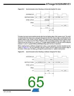
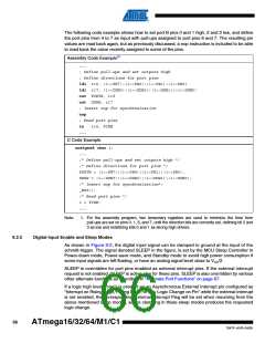
9.3.1
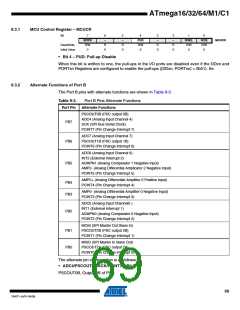
MCU Control Register – MCUCR
Bit
7
SPIPS
R/W
0
6
–
5
–
4
3
–
2
–
1
IVSEL
R/W
0
0
IVCE
R/W
0
PUD
R/W
0
MCUCR
Read/Write
Initial Value
R
0
R
0
R
0
R
0
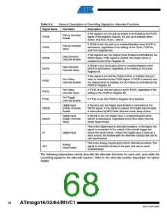
• Bit 4 – PUD: Pull-up Disable
When this bit is written to one, the pull-ups in the I/O ports are disabled even if the DDxn and
PORTxn Registers are configured to enable the pull-ups ({DDxn, PORTxn} = 0b01). Se
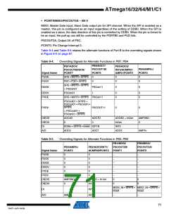
9.3.2
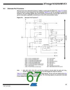
Alternate Functions of Port B
The Port B pins with alternate functions are shown in Table 9-3.
Table 9-3.
Port Pin
Port B Pins Alternate Functions
Alternate Functions
PSCOUT0B (PSC output 0B)
ADC4 (Analog Input Channel 4)
SCK (SPI Bus Serial Clock)
PB7
PB6
PCINT7 (Pin Change Interrupt 7)
ADC7 (Analog Input Channel 7)
PSCOUT1B (PSC output 1B)
PCINT6 (Pin Change Interrupt 6)
ADC6 (Analog Input Channel 6)
INT2 (External Interrupt 2)
PB5
ACMPN1 (Analog Comparator 1 Negative Input)
AMP2- (Analog Differential Amplicator 2 Negative Input)
PCINT5 (Pin Change Interrupt 5)
AMP0+ (Analog Differential Amplifier 0 Positive Input)
PCINT4 (Pin Change Interrupt 4)
PB4
PB3
AMP0- (Analog Differential Amplifier 0 Negative Input)
PCINT3 (Pin Change Interrupt 3)
ADC5 (Analog Input Channel5 )
INT1 (External Interrupt 1)
PB2
ACMPN0 (Analog Comparator 0 Negative Input)
PCINT2 (Pin Change Interrupt 2)
MOSI (SPI Master Out Slave In)
PSCOUT2B (PSC output 2B)
PCINT1 (Pin Change Interrupt 1)
PB1
PB0
MISO (SPI Master In Slave Out)
PSCOUT2A (PSC output 2A)
PCINT0 (Pin Change Interrupt 0)
The alternate pin configuration is as follows:
• ADC4/PSCOUT0B/SCK/PCINT7 – Bit 7
PSCOUT0B, Output 0B of PSC.
69
7647F–AVR–04/09

 ATMEL [ ATMEL ]