ATmega16/32/64/M1/C1
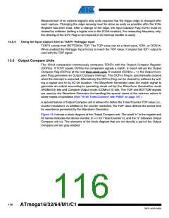
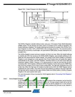
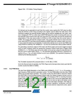
Figure 13-4. Output Compare Unit, Block Diagram
DATA BUS (8-bit)
TEMP (8-bit)
OCRnxH Buf. (8-bit)
OCRnxL Buf. (8-bit)
TCNTnH (8-bit)
TCNTnL (8-bit)
OCRnx Buffer (16-bit Register)
TCNTn (16-bit Counter)
OCRnxH (8-bit)
OCRnxL (8-bit)
OCRnx (16-bit Register)
=
(16-bit Comparator )
OCFnx (Int.Req.)
TOP
OCnx
Waveform Generator
BOTTOM
WGMn3:0
COMnx1:0
The OCRnx Register is double buffered when using any of the twelve Pulse Width Modulation
(PWM) modes. For the Normal and Clear Timer on Compare (CTC) modes of operation, the
double buffering is disabled. The double buffering synchronizes the update of the OCRnx Com-
pare Register to either TOP or BOTTOM of the counting sequence. The synchronization
prevents the occurrence of odd-length, non-symmetrical PWM pulses, thereby making the out-
put glitch-free.
The OCRnx Register access may seem complex, but this is not case. When the double buffering
is enabled, the CPU has access to the OCRnx Buffer Register, and if double buffering is dis-
abled the CPU will access the OCRnx directly. The content of the OCR1x (Buffer or Compare)
Register is only changed by a write operation (the Timer/Counter does not update this register
automatically as the TCNT1 and ICR1 Register). Therefore OCR1x is not read via the high byte
temporary register (TEMP). However, it is a good practice to read the low byte first as when
accessing other 16-bit registers. Writing the OCRnx Registers must be done via the TEMP Reg-
ister since the compare of all 16 bits is done continuously. The high byte (OCRnxH) has to be
written first. When the high byte I/O location is written by the CPU, the TEMP Register will be
updated by the value written. Then when the low byte (OCRnxL) is written to the lower eight bits,
the high byte will be copied into the upper 8-bits of either the OCRnx buffer or OCRnx Compare
Register in the same system clock cycle.
For more information of how to access the 16-bit registers refer to “Accessing 16-bit Registers”
on page 109.
13.6.1
Force Output Compare
In non-PWM Waveform Generation modes, the match output of the comparator can be forced by
writing a one to the Force Output Compare (FOCnx) bit. Forcing compare match will not set the
OCFnx Flag or reload/clear the timer, but the OCnx pin will be updated as if a real compare
match had occurred (the COMn1:0 bits settings define whether the OCnx pin is set, cleared or
toggled).
117
7647F–AVR–04/09

 ATMEL [ ATMEL ]