ATmega48/88/168
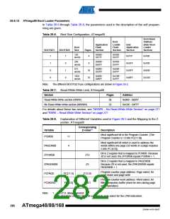
shown below. Refer to Table 27-6 on page 288 for detailed description and mapping of the Fuse
High byte.
Bit
Rd
7
6
5
4
3
2
1
0
FHB7
FHB6
FHB5
FHB4
FHB3
FHB2
FHB1
FHB0
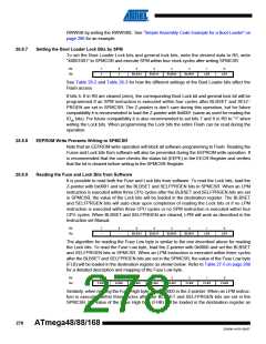
When reading the Extended Fuse byte, load 0x0002 in the Z-pointer. When an LPM instruction
is executed within three cycles after the BLBSET and SELFPRGEN bits are set in the SPMCSR,
the value of the Extended Fuse byte (EFB) will be loaded in the destination register as shown
below. Refer to Table 27-4 on page 287 for detailed description and mapping of the Extended
Fuse byte.
Bit
Rd
7
6
5
4
3
2
1
0
–
–
–
–
EFB3
EFB2
EFB1
EFB0
Fuse and Lock bits that are programmed, will be read as zero. Fuse and Lock bits that are
unprogrammed, will be read as one.
26.8.10 Preventing Flash Corruption
During periods of low VCC, the Flash program can be corrupted because the supply voltage is
too low for the CPU and the Flash to operate properly. These issues are the same as for board
level systems using the Flash, and the same design solutions should be applied.
A Flash program corruption can be caused by two situations when the voltage is too low. First, a
regular write sequence to the Flash requires a minimum voltage to operate correctly. Secondly,
the CPU itself can execute instructions incorrectly, if the supply voltage for executing instructions
is too low.
Flash corruption can easily be avoided by following these design recommendations (one is
sufficient):
1. If there is no need for a Boot Loader update in the system, program the Boot Loader Lock
bits to prevent any Boot Loader software updates.
2. Keep the AVR RESET active (low) during periods of insufficient power supply voltage.
This can be done by enabling the internal Brown-out Detector (BOD) if the operating volt-
age matches the detection level. If not, an external low VCC reset protection circuit can be
used. If a reset occurs while a write operation is in progress, the write operation will be
completed provided that the power supply voltage is sufficient.
3. Keep the AVR core in Power-down sleep mode during periods of low VCC. This will pre-
vent the CPU from attempting to decode and execute instructions, effectively protecting
the SPMCSR Register and thus the Flash from unintentional writes.
279
2545M–AVR–09/07

 ATMEL [ ATMEL ]