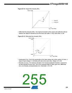
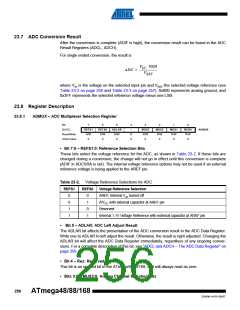
ATmega48/88/168
23.8.3
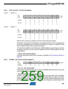
ADCL and ADCH – The ADC Data Register
23.8.3.1
ADLAR = 0
Bit
15
14
13
12
11
10
9
8
(0x79)
(0x78)
–
–
–
–
–
–
ADC9
ADC8
ADCH
ADCL
ADC7
ADC6
ADC5
ADC4
ADC3
ADC2
ADC1
ADC0
7
R
R
0
6
R
R
0
5
R
R
0
4
R
R
0
3
R
R
0
2
R
R
0
1
R
R
0
0
R
R
0
Read/Write
Initial Value
0
0
0
0
0
0
0
0
23.8.3.2
ADLAR = 1
Bit
15
14
13
12
11
10
9
8
(0x79)
(0x78)
ADC9
ADC8
ADC7
ADC6
ADC5
ADC4
ADC3
ADC2
ADCH
ADCL
ADC1
ADC0
–
5
–
4
–
3
–
2
–
1
–
0
7
R
R
0
6
R
R
0
Read/Write
Initial Value
R
R
0
R
R
0
R
R
0
R
R
0
R
R
0
R
R
0
0
0
0
0
0
0
0
0
When an ADC conversion is complete, the result is found in these two registers.
When ADCL is read, the ADC Data Register is not updated until ADCH is read. Consequently, if
the result is left adjusted and no more than 8-bit precision is required, it is sufficient to read
ADCH. Otherwise, ADCL must be read first, then ADCH.
The ADLAR bit in ADMUX, and the MUXn bits in ADMUX affect the way the result is read from
the registers. If ADLAR is set, the result is left adjusted. If ADLAR is cleared (default), the result
is right adjusted.
• ADC9:0: ADC Conversion Result
These bits represent the result from the conversion, as detailed in “ADC Conversion Result” on
page 256.
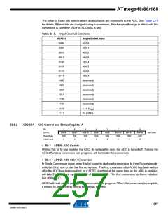
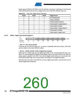
23.8.4
ADCSRB – ADC Control and Status Register B
Bit
7
–
6
ACME
R/W
0
5
–
4
–
3
–
2
ADTS2
R/W
0
1
ADTS1
R/W
0
0
ADTS0
R/W
0
(0x7B)
ADCSRB
Read/Write
Initial Value
R
0
R
0
R
0
R
0
• Bit 7, 5:3 – Res: Reserved Bits
These bits are reserved for future use. To ensure compatibility with future devices, these bist
must be written to zero when ADCSRB is written.
• Bit 2:0 – ADTS2:0: ADC Auto Trigger Source
If ADATE in ADCSRA is written to one, the value of these bits selects which source will trigger
an ADC conversion. If ADATE is cleared, the ADTS2:0 settings will have no effect. A conversion
will be triggered by the rising edge of the selected Interrupt Flag. Note that switching from a trig-
ger source that is cleared to a trigger source that is set, will generate a positive edge on the
259
2545M–AVR–09/07

 ATMEL [ ATMEL ]