23.7 ADC Conversion Result
After the conversion is complete (ADIF is high), the conversion result can be found in the ADC
Result Registers (ADCL, ADCH).
For single ended conversion, the result is
V
⋅ 1024
IN
ADC = --------------------------
V
REF
where VIN is the voltage on the selected input pin and VREF the selected voltage reference (see
Table 23-2 on page 256 and Table 23-3 on page 257). 0x000 represents analog ground, and
0x3FF represents the selected reference voltage minus one LSB.
23.8 Register Description
23.8.1
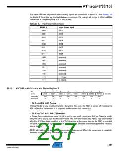
ADMUX – ADC Multiplexer Selection Register
Bit
7
REFS1
R/W
0
6
REFS0
R/W
0
5
ADLAR
R/W
0
4
–
3
MUX3
R/W
0
2
MUX2
R/W
0
1
MUX1
R/W
0
0
MUX0
R/W
0
(0x7C)
ADMUX
Read/Write
Initial Value
R
0
• Bit 7:6 – REFS1:0: Reference Selection Bits
These bits select the voltage reference for the ADC, as shown in Table 23-2. If these bits are
changed during a conversion, the change will not go in effect until this conversion is complete
(ADIF in ADCSRA is set). The internal voltage reference options may not be used if an external
reference voltage is being applied to the AREF pin.
Table 23-2. Voltage Reference Selections for ADC
REFS1
REFS0
Voltage Reference Selection
0
0
1
1
0
1
0
1
AREF, Internal Vref turned off
AVCC with external capacitor at AREF pin
Reserved
Internal 1.1V Voltage Reference with external capacitor at AREF pin
•
Bit 5 – ADLAR: ADC Left Adjust Result
The ADLAR bit affects the presentation of the ADC conversion result in the ADC Data Register.
Write one to ADLAR to left adjust the result. Otherwise, the result is right adjusted. Changing the
ADLAR bit will affect the ADC Data Register immediately, regardless of any ongoing conver-
sions. For a complete description of this bit, see “ADCL and ADCH – The ADC Data Register” on
page 259.
• Bit 4 – Res: Reserved Bit
This bit is an unused bit in the ATmega48/88/168, and will always read as zero.
• Bits 3:0 – MUX3:0: Analog Channel Selection Bits
256
ATmega48/88/168
2545M–AVR–09/07

 ATMEL [ ATMEL ]