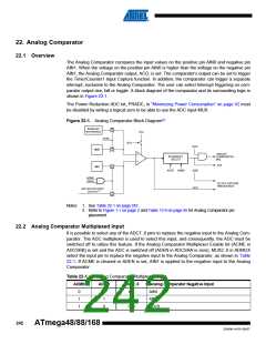
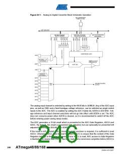
Figure 23-1. Analog to Digital Converter Block Schematic Operation
ADC CONVERSION
COMPLETE IRQ
8-BIT DATA BUS
15
0
ADC MULTIPLEXER
SELECT (ADMUX)
ADC DATA REGISTER
(ADCH/ADCL)
ADC CTRL. & STATUS
REGISTER (ADCSRA)
MUX DECODER
PRESCALER
CONVERSION LOGIC
AVCC
INTERNAL 1.1V
REFERENCE
SAMPLE & HOLD
COMPARATOR
AREF
GND
10-BIT DAC
-
+
BANDGAP
REFERENCE
ADC7
ADC6
ADC5
ADC4
ADC3
ADC2
ADC1
ADC0
ADC MULTIPLEXER
OUTPUT
INPUT
MUX
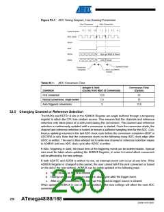
The analog input channel is selected by writing to the MUX bits in ADMUX. Any of the ADC input
pins, as well as GND and a fixed bandgap voltage reference, can be selected as single ended
inputs to the ADC. The ADC is enabled by setting the ADC Enable bit, ADEN in ADCSRA. Volt-
age reference and input channel selections will not go into effect until ADEN is set. The ADC
does not consume power when ADEN is cleared, so it is recommended to switch off the ADC
before entering power saving sleep modes.
The ADC generates a 10-bit result which is presented in the ADC Data Registers, ADCH and
ADCL. By default, the result is presented right adjusted, but can optionally be presented left
adjusted by setting the ADLAR bit in ADMUX.
If the result is left adjusted and no more than 8-bit precision is required, it is sufficient to read
ADCH. Otherwise, ADCL must be read first, then ADCH, to ensure that the content of the Data
Registers belongs to the same conversion. Once ADCL is read, ADC access to Data Registers
is blocked. This means that if ADCL has been read, and a conversion completes before ADCH is
246
ATmega48/88/168
2545M–AVR–09/07

 ATMEL [ ATMEL ]