will be the same, but TOP should be replaced by BOTTOM, TOP-1 by BOTTOM+1 and so on.
The same renaming applies for modes that set the TOV1 Flag at BOTTOM.
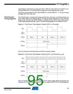
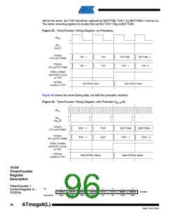
Figure 43. Timer/Counter Timing Diagram, no Prescaling
clkI/O
clkTn
(clkI/O/1)
TCNTn
TOP - 1
TOP - 1
TOP
TOP
BOTTOM
TOP - 1
BOTTOM + 1
TOP - 2
(CTC and FPWM)
TCNTn
(PC and PFC PWM)
TOVn (FPWM)
and ICFn (if used
as TOP)
OCRnx
(Update at TOP)
Old OCRnx Value
New OCRnx Value
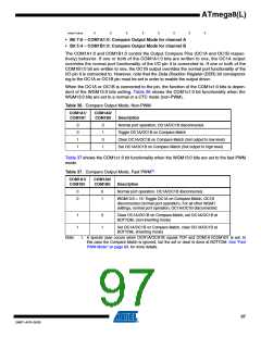
Figure 44 shows the same timing data, but with the prescaler enabled.
Figure 44. Timer/Counter Timing Diagram, with Prescaler (fclk_I/O/8)
clkI/O
clkTn
(clkI/O/8)
TCNTn
TOP - 1
TOP - 1
TOP
TOP
BOTTOM
TOP - 1
BOTTOM + 1
TOP - 2
(CTC and FPWM)
TCNTn
(PC and PFC PWM)
TOVn (FPWM)
and ICFn (if used
as TOP)
OCRnx
(Update at TOP)
Old OCRnx Value
New OCRnx Value
16-bit
Timer/Counter
Register
Description
Timer/Counter 1
Control Register A –
TCCR1A
Bit
7
6
5
4
3
FOC1A
W
2
FOC1B
W
1
0
COM1A1
COM1A0
R/W
COM1B1
R/W
COM1B0
R/W
WGM11
R/W
WGM10
R/W
TCCR1A
Read/Write
R/W
96
ATmega8(L)
2486T–AVR–05/08

 ATMEL [ ATMEL ]