ATmega8(L)
Programming the
Flash
The Flash is organized in pages, see Table 89 on page 225. When programming the Flash, the
program data is latched into a page buffer. This allows one page of program data to be pro-
grammed simultaneously. The following procedure describes how to program the entire Flash
memory:
A. Load Command “Write Flash”
1. Set XA1, XA0 to “10”. This enables command loading.
2. Set BS1 to ”0”.
3. Set DATA to “0001 0000”. This is the command for Write Flash.
4. Give XTAL1 a positive pulse. This loads the command.
B. Load Address Low byte
1. Set XA1, XA0 to “00”. This enables address loading.
2. Set BS1 to “0”. This selects low address.
3. Set DATA = Address Low byte (0x00 - 0xFF).
4. Give XTAL1 a positive pulse. This loads the address Low byte.
C. Load Data Low byte
1. Set XA1, XA0 to “01”. This enables data loading.
2. Set DATA = Data Low byte (0x00 - 0xFF).
3. Give XTAL1 a positive pulse. This loads the data byte.
D. Load Data High byte
1. Set BS1 to “1”. This selects high data byte.
2. Set XA1, XA0 to “01”. This enables data loading.
3. Set DATA = Data High byte (0x00 - 0xFF).
4. Give XTAL1 a positive pulse. This loads the data byte.
E. Latch Data
1. Set BS1 to “1”. This selects high data byte.
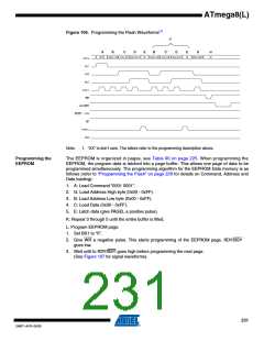
2. Give PAGEL a positive pulse. This latches the data bytes. (See Figure 106 for signal
waveforms)
F. Repeat B through E until the entire buffer is filled or until all data within the page is loaded.
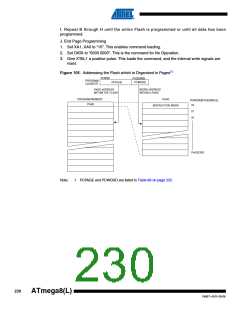
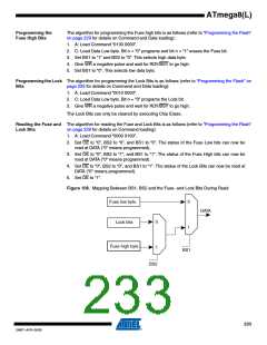
While the lower bits in the address are mapped to words within the page, the higher bits address
the pages within the FLASH. This is illustrated in Figure 105 on page 230. Note that if less than
eight bits are required to address words in the page (pagesize < 256), the most significant bit(s)
in the address Low byte are used to address the page when performing a page write.
G. Load Address High byte
1. Set XA1, XA0 to “00”. This enables address loading.
2. Set BS1 to “1”. This selects high address.
3. Set DATA = Address High byte (0x00 - 0xFF).
4. Give XTAL1 a positive pulse. This loads the address High byte.
H. Program Page
1. Set BS1 = “0”
2. Give WR a negative pulse. This starts programming of the entire page of data. RDY/BSY
goes low.
3. Wait until RDY/BSY goes high. (See Figure 106 for signal waveforms)
229
2486T–AVR–05/08

 ATMEL [ ATMEL ]