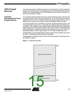
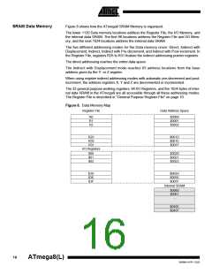
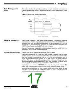
ATmega8(L)
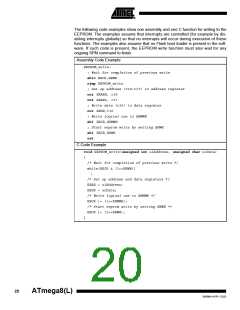
value into the EEPROM. The EEMWE bit must be written to one before a logical one is
written to EEWE, otherwise no EEPROM write takes place. The following procedure
should be followed when writing the EEPROM (the order of steps 3 and 4 is not
essential):
1. Wait until EEWE becomes zero.
2. Wait until SPMEN in SPMCR becomes zero.
3. Write new EEPROM address to EEAR (optional).
4. Write new EEPROM data to EEDR (optional).
5. Write a logical one to the EEMWE bit while writing a zero to EEWE in EECR.
6. Within four clock cycles after setting EEMWE, write a logical one to EEWE.
The EEPROM can not be programmed during a CPU write to the Flash memory. The
software must check that the Flash programming is completed before initiating a new
EEPROM write. Step 2 is only relevant if the software contains a boot loader allowing
the CPU to program the Flash. If the Flash is never being updated by the CPU, step 2
can be omitted. See “Boot Loader Support – Read-While-Write Self-Programming” on
page 206 for details about boot programming.
Caution: An interrupt between step 5 and step 6 will make the write cycle fail, since the
EEPROM Master Write Enable will time-out. If an interrupt routine accessing the
EEPROM is interrupting another EEPROM access, the EEAR or EEDR Register will be
modified, causing the interrupted EEPROM access to fail. It is recommended to have
the Global Interrupt Flag cleared during all the steps to avoid these problems.
When the write access time has elapsed, the EEWE bit is cleared by hardware. The
user software can poll this bit and wait for a zero before writing the next byte. When
EEWE has been set, the CPU is halted for two cycles before the next instruction is
executed.
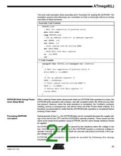
• Bit 0 – EERE: EEPROM Read Enable
The EEPROM Read Enable Signal EERE is the read strobe to the EEPROM. When the
correct address is set up in the EEAR Register, the EERE bit must be written to a logic
one to trigger the EEPROM read. The EEPROM read access takes one instruction, and
the requested data is available immediately. When the EEPROM is read, the CPU is
halted for four cycles before the next instruction is executed.
The user should poll the EEWE bit before starting the read operation. If a write operation
is in progress, it is neither possible to read the EEPROM, nor to change the EEAR
Register.
The calibrated Oscillator is used to time the EEPROM accesses. Table 1 lists the typical
programming time for EEPROM access from the CPU.
Table 1. EEPROM Programming Time
Number of Calibrated RC
Symbol
Oscillator Cycles(1)
Typ Programming Time
EEPROM Write (from CPU)
8448
8.5 ms
Note:
1. Uses 1 MHz clock, independent of CKSEL Fuse settings.
19
2486M–AVR–12/03

 ATMEL [ ATMEL ]