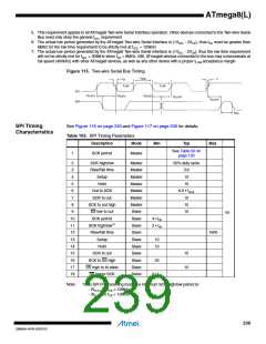
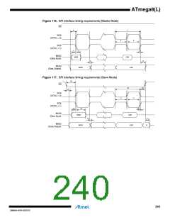
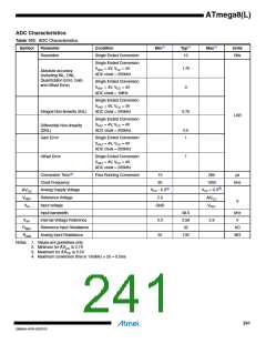
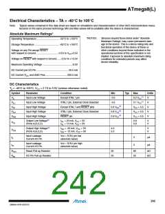
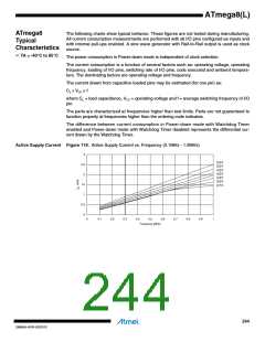
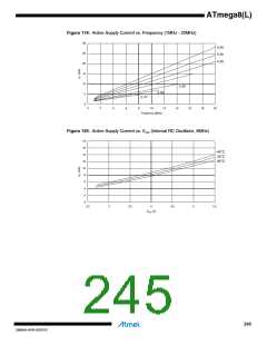
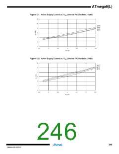
ATmega8(L)
DC Characteristics
TA = -40C to 105C, VCC = 2.7V to 5.5V (unless otherwise noted) (Continued)
Symbol
Parameter
Condition
Min
Typ
Max
Units
Active 4 MHz, VCC = 3V
(ATmega8L)
6
mA
Active 8 MHz, VCC = 5V
(ATmega8)
15
3
mA
mA
mA
Power Supply Current
Idle 4 MHz, VCC = 3V
(ATmega8L)
ICC
Idle 8 MHz, VCC = 5V
(ATmega8)
8
WDT enabled, VCC = 3V
WDT disabled, VCC = 3V
35
6
µA
µA
Power-down mode(5)
Analog Comparator
Input Offset Voltage
VCC = 5V
Vin = VCC/2
VACIO
IACLK
tACPD
20
50
mV
nA
ns
Analog Comparator
Input Leakage Current
VCC = 5V
Vin = VCC/2
-50
Analog Comparator
Propagation Delay
VCC = 2.7V
VCC = 5.0V
750
500
Notes: 1. “Max” means the highest value where the pin is guaranteed to be read as low
2. “Min” means the lowest value where the pin is guaranteed to be read as high
3. Although each I/O port can sink more than the test conditions (20mA at Vcc = 5V, 10mA at Vcc = 3V) under steady state
conditions (non-transient), the following must be observed:
PDIP Package:
1] The sum of all IOL, for all ports, should not exceed 400 mA.
2] The sum of all IOL, for ports C0 - C5 should not exceed 200 mA.
3] The sum of all IOL, for ports B0 - B7, C6, D0 - D7 and XTAL2, should not exceed 100 mA.
TQFP and MLF Package:
1] The sum of all IOL, for all ports, should not exceed 400 mA.
2] The sum of all IOL, for ports C0 - C5, should not exceed 200 mA.
3] The sum of all IOL, for ports C6, D0 - D4, should not exceed 300 mA.
4] The sum of all IOL, for ports B0 - B7, D5 - D7, should not exceed 300 mA.
If IOL exceeds the test condition, VOL may exceed the related specification. Pins are not guaranteed to sink current greater
than the listed test condition.
4. Although each I/O port can source more than the test conditions (20mA at Vcc = 5V, 10mA at Vcc = 3V) under steady state
conditions (non-transient), the following must be observed:
PDIP Package:
1] The sum of all IOH, for all ports, should not exceed 400 mA.
2] The sum of all IOH, for port C0 - C5, should not exceed 100 mA.
3] The sum of all IOH, for ports B0 - B7, C6, D0 - D7 and XTAL2, should not exceed 100 mA.
TQFP and MLF Package:
1] The sum of all IOH, for all ports, should not exceed 400 mA.
2] The sum of all IOH, for ports C0 - C5, should not exceed 200 mA.
3] The sum of all IOH, for ports C6, D0 - D4, should not exceed 300 mA.
4] The sum of all IOH, for ports B0 - B7, D5 - D7, should not exceed 300 mA.
If IOH exceeds the test condition, VOH may exceed the related specification. Pins are not guaranteed to source current
greater than the listed test condition.
5. Minimum VCC for Power-down is 2.5V.
243
2486AA–AVR–02/2013

 ATMEL [ ATMEL ]