ATmega8(L)
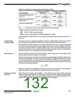
Table 52. Equations for Calculating Baud Rate Register Setting
Equation for Calculating
Baud Rate(1)
Equation for Calculating
UBRR Value
Operating Mode
Asynchronous Normal mode
(U2X = 0)
f
OSC
f
OSC
BAUD = --------------------------------------
UBRR = ----------------------- – 1
16BAUD
16UBRR + 1
Asynchronous Double Speed
Mode (U2X = 1)
f
OSC
f
OSC
BAUD = -----------------------------------
UBRR = -------------------- – 1
8UBRR + 1
8BAUD
Synchronous Master Mode
f
OSC
f
OSC
BAUD = -----------------------------------
UBRR = -------------------- – 1
2UBRR + 1
2BAUD
Note:
1. The baud rate is defined to be the transfer rate in bit per second (bps)
BAUD Baud rate (in bits per second, bps)
fOSC System Oscillator clock frequency
UBRR Contents of the UBRRH and UBRRL Registers (0 - 4095)
Some examples of UBRR values for some system clock frequencies are found in Table 60 on
page 153.
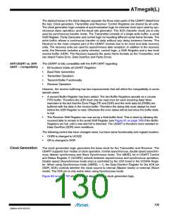
Double Speed
Operation (U2X)
The transfer rate can be doubled by setting the U2X bit in UCSRA. Setting this bit only has effect
for the asynchronous operation. Set this bit to zero when using synchronous operation.
Setting this bit will reduce the divisor of the baud rate divider from 16 to 8, effectively doubling
the transfer rate for asynchronous communication. Note however that the Receiver will in this
case only use half the number of samples (reduced from 16 to 8) for data sampling and clock
recovery, and therefore a more accurate baud rate setting and system clock are required when
this mode is used. For the Transmitter, there are no downsides.
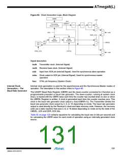
External Clock
External clocking is used by the Synchronous Slave modes of operation. The description in this
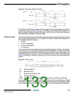
section refers to Figure 62 on page 131 for details.
External clock input from the XCK pin is sampled by a synchronization register to minimize the
chance of meta-stability. The output from the synchronization register must then pass through
an edge detector before it can be used by the Transmitter and Receiver. This process intro-
duces a two CPU clock period delay and therefore the maximum external XCK clock frequency
is limited by the following equation:
f
OSC
-----------
f
XCK
4
Note that fosc depends on the stability of the system clock source. It is therefore recommended to
add some margin to avoid possible loss of data due to frequency variations.
Synchronous Clock
Operation
When Synchronous mode is used (UMSEL = 1), the XCK pin will be used as either clock input
(Slave) or clock output (Master). The dependency between the clock edges and data sampling
or data change is the same. The basic principle is that data input (on RxD) is sampled at the
opposite XCK clock edge of the edge the data output (TxD) is changed.
132
2486AA–AVR–02/2013

 ATMEL [ ATMEL ]