ATmega8(L)
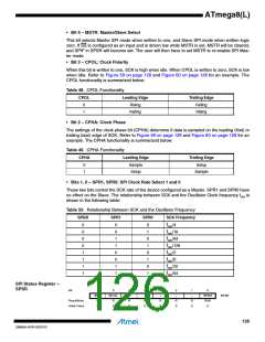
• Bit 7 – SPIF: SPI Interrupt Flag
When a serial transfer is complete, the SPIF Flag is set. An interrupt is generated if SPIE in
SPCR is set and global interrupts are enabled. If SS is an input and is driven low when the SPI is
in Master mode, this will also set the SPIF Flag. SPIF is cleared by hardware when executing the
corresponding interrupt Handling Vector. Alternatively, the SPIF bit is cleared by first reading the
SPI Status Register with SPIF set, then accessing the SPI Data Register (SPDR).
• Bit 6 – WCOL: Write COLlision Flag
The WCOL bit is set if the SPI Data Register (SPDR) is written during a data transfer. The
WCOL bit (and the SPIF bit) are cleared by first reading the SPI Status Register with WCOL set,
and then accessing the SPI Data Register.
• Bit 5..1 – Res: Reserved Bits
These bits are reserved bits in the ATmega8 and will always read as zero.
• Bit 0 – SPI2X: Double SPI Speed Bit
When this bit is written logic one the SPI speed (SCK Frequency) will be doubled when the SPI
is in Master mode (see Table 50 on page 126). This means that the minimum SCK period will be
2 CPU clock periods. When the SPI is configured as Slave, the SPI is only guaranteed to work at
fosc/4 or lower.
The SPI interface on the ATmega8 is also used for Program memory and EEPROM download-
ing or uploading. See page 230 for Serial Programming and verification.
SPI Data Register –
SPDR
Bit
7
6
5
4
3
2
1
0
MSB
R/W
X
LSB
R/W
X
SPDR
Read/Write
Initial Value
R/W
X
R/W
X
R/W
X
R/W
X
R/W
X
R/W
X
Undefined
The SPI Data Register is a Read/Write Register used for data transfer between the Register File
and the SPI Shift Register. Writing to the register initiates data transmission. Reading the regis-
ter causes the Shift Register Receive buffer to be read.
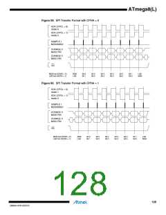
Data Modes
There are four combinations of SCK phase and polarity with respect to serial data, which are
determined by control bits CPHA and CPOL. The SPI data transfer formats are shown in Figure
59 on page 128 and Figure 60 on page 128. Data bits are shifted out and latched in on opposite
edges of the SCK signal, ensuring sufficient time for data signals to stabilize. This is clearly seen
by summarizing Table 48 on page 126 and Table 49 on page 126, as done below:
Table 51. CPOL and CPHA Functionality
Leading Edge
Sample (Rising)
Setup (Rising)
Sample (Falling)
Setup (Falling)
Trailing Edge
Setup (Falling)
Sample (Falling)
Setup (Rising)
Sample (Rising)
SPI Mode
CPOL = 0, CPHA = 0
CPOL = 0, CPHA = 1
CPOL = 1, CPHA = 0
CPOL = 1, CPHA = 1
0
1
2
3
127
2486AA–AVR–02/2013

 ATMEL [ ATMEL ]