ATmega8(L)
• Bit 4 – MSTR: Master/Slave Select
This bit selects Master SPI mode when written to one, and Slave SPI mode when written logic
zero. If SS is configured as an input and is driven low while MSTR is set, MSTR will be cleared,
and SPIF in SPSR will become set. The user will then have to set MSTR to re-enable SPI Mas-
ter mode.
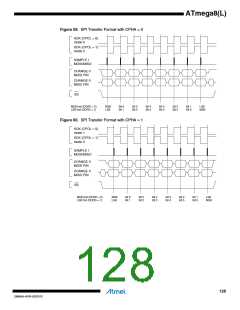
• Bit 3 – CPOL: Clock Polarity
When this bit is written to one, SCK is high when idle. When CPOL is written to zero, SCK is low
when idle. Refer to Figure 59 on page 128 and Figure 60 on page 128 for an example. The
CPOL functionality is summarized below:
Table 48. CPOL Functionality
CPOL
Leading Edge
Rising
Trailing Edge
Falling
0
1
Falling
Rising
• Bit 2 – CPHA: Clock Phase
The settings of the clock phase bit (CPHA) determine if data is sampled on the leading (first) or
trailing (last) edge of SCK. Refer to Figure 59 on page 128 and Figure 60 on page 128 for an
example. The CPHA functionality is summarized below:
Table 49. CPHA Functionality
CPHA
Leading Edge
Sample
Trailing Edge
Setup
0
1
Setup
Sample
• Bits 1, 0 – SPR1, SPR0: SPI Clock Rate Select 1 and 0
These two bits control the SCK rate of the device configured as a Master. SPR1 and SPR0 have
no effect on the Slave. The relationship between SCK and the Oscillator Clock frequency fosc is
shown in the following table:
Table 50. Relationship Between SCK and the Oscillator Frequency
SPI2X
SPR1
SPR0
SCK Frequency
fosc/4
0
0
0
0
1
1
1
1
0
0
1
1
0
0
1
1
0
1
0
1
0
1
0
1
fosc/16
fosc/64
fosc/128
fosc/2
fosc/8
fosc/32
fosc/64
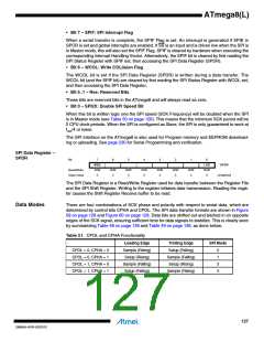
SPI Status Register –
SPSR
Bit
7
SPIF
R
6
5
–
4
–
3
–
2
–
1
–
0
SPI2X
R/W
0
WCOL
SPSR
Read/Write
Initial Value
R
0
R
0
R
0
R
0
R
0
R
0
0
126
2486AA–AVR–02/2013

 ATMEL [ ATMEL ]