PDF
最近搜索
热门搜索
发布采购

| 型号: | ATMEGA64L-8AU |
| PDF下载: | 下载PDF文件 查看货源 |
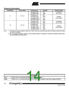
| 内容描述: | 8位微控制器,带有64K字节的系统内可编程闪存 [8-bit Microcontroller with 64K Bytes In-System Programmable Flash] |
| 分类和应用: | 闪存微控制器和处理器外围集成电路异步传输模式PCATM时钟 |
| 文件页数/大小: | 23 页 / 287 K |
| 品牌: |  ATMEL [ ATMEL ] ATMEL [ ATMEL ] |
专业IC领域供求交易平台:提供全面的IC Datasheet资料和资讯,Datasheet 1000万数据,IC品牌1000多家。