Setting the Boot Loader Lock To set the Boot Loader Lock bits, write the desired data to R0, write “X0001001” to
Bits by SPM
SPMCSR and execute SPM within four clock cycles after writing SPMCSR. The only
accessible Lock bits are the Boot Lock bits that may prevent the Application and Boot
Loader section from any software update by the MCU.
Bit
R0
7
6
5
4
3
2
1
0
1
1
BLB12
BLB11
BLB02
BLB01
1
1
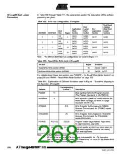
See Table 105 and Table 106 for how the different settings of the Boot Loader bits affect
the Flash access.
If bits 5..2 in R0 are cleared (zero), the corresponding Boot Lock bit will be programmed
if an SPM instruction is executed within four cycles after BLBSET and SELFPRGEN are
set in SPMCSR. The Z-pointer is don’t care during this operation, but for future compat-
ibility it is recommended to load the Z-pointer with 0x0001 (same as used for reading the
lOck bits). For future compatibility it is also recommended to set bits 7, 6, 1, and 0 in R0
to “1” when writing the Lock bits. When programming the Lock bits the entire Flash can
be read during the operation.
EEPROM Write Prevents
Writing to SPMCSR
Note that an EEPROM write operation will block all software programming to Flash.
Reading the Fuses and Lock bits from software will also be prevented during the
EEPROM write operation. It is recommended that the user checks the status bit (EEPE)
in the EECR Register and verifies that the bit is cleared before writing to the SPMCSR
Register.
Reading the Fuse and Lock
Bits from Software
It is possible to read both the Fuse and Lock bits from software. To read the Lock bits,
load the Z-pointer with 0x0001 and set the BLBSET and SELFPRGEN bits in SPMCSR.
When an LPM instruction is executed within three CPU cycles after the BLBSET and
SELFPRGEN bits are set in SPMCSR, the value of the Lock bits will be loaded in the
destination register. The BLBSET and SELFPRGEN bits will auto-clear upon completion
of reading the Lock bits or if no LPM instruction is executed within three CPU cycles or
no SPM instruction is executed within four CPU cycles. When BLBSET and SELF-
PRGEN are cleared, LPM will work as described in the Instruction set Manual.
Bit
Rd
7
6
5
4
3
2
1
0
–
–
BLB12
BLB11
BLB02
BLB01
LB2
LB1
The algorithm for reading the Fuse Low byte is similar to the one described above for
reading the Lock bits. To read the Fuse Low byte, load the Z-pointer with 0x0000 and
set the BLBSET and SELFPRGEN bits in SPMCSR. When an LPM instruction is exe-
cuted within three cycles after the BLBSET and SELFPRGEN bits are set in the
SPMCSR, the value of the Fuse Low byte (FLB) will be loaded in the destination register
as shown below. Refer to Table 119 on page 272 for a detailed description and mapping
of the Fuse Low byte.
Bit
Rd
7
6
5
4
3
2
1
0
FLB7
FLB6
FLB5
FLB4
FLB3
FLB2
FLB1
FLB0
Similarly, when reading the Fuse High byte, load 0x0003 in the Z-pointer. When an LPM
instruction is executed within three cycles after the BLBSET and SELFPRGEN bits are
set in the SPMCSR, the value of the Fuse High byte (FHB) will be loaded in the destina-
tion register as shown below. Refer to Table 120 on page 273 for detailed description
and mapping of the Fuse High byte.
Bit
Rd
7
6
5
4
3
2
1
0
FHB7
FHB6
FHB5
FHB4
FHB3
FHB2
FHB1
FHB0
264
ATmega48/88/168
2545D–AVR–07/04

 ATMEL [ ATMEL ]